

- 中文
- English
- Español
The world's first! 100mm diamond wafer is available!
2023-12-07 16:35:47
Click:
“
Recently, Diamond Foundry Inc, headquartered in San Francisco, California, announced that it has produced the world’s first single-crystal diamond wafer with a diameter of 100 mm. The company plans to offer diamond substrates as a way to improve thermal performance, which in turn could improve artificial intelligence computing and wireless communications as well as smaller power electronics devices.
”
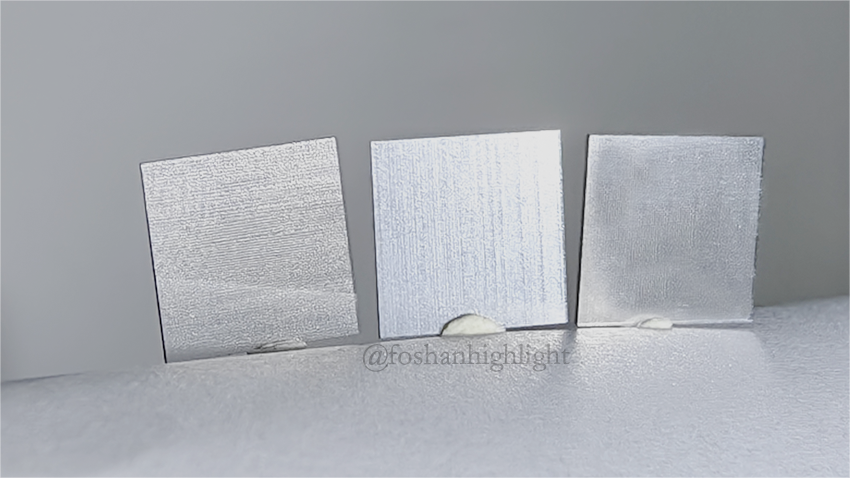
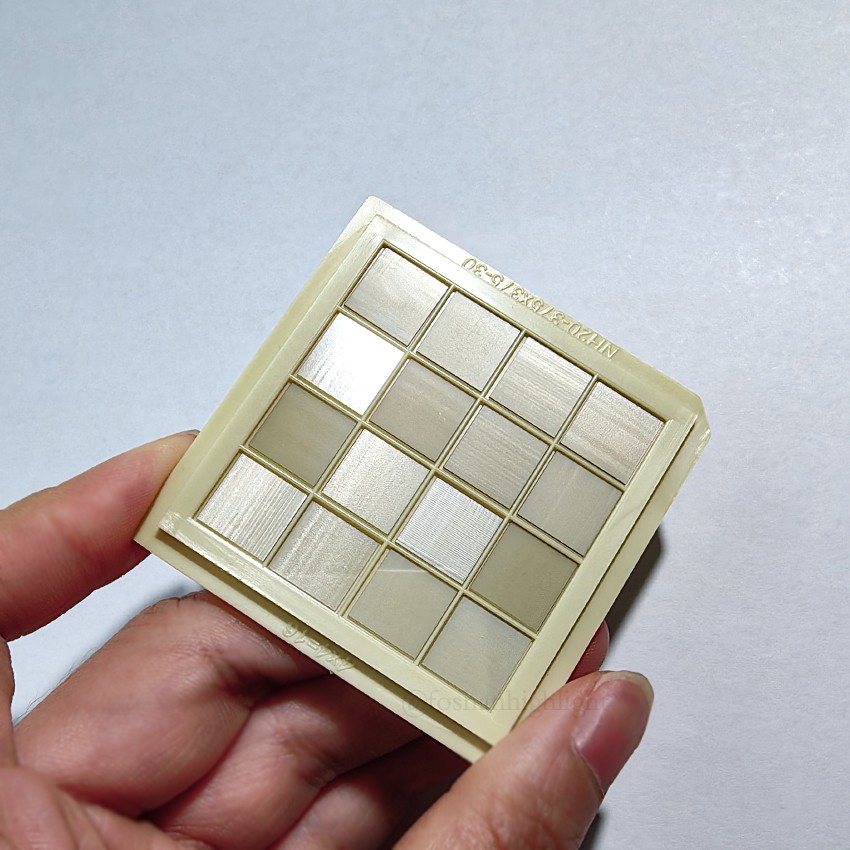
Recently, Diamond Foundry Inc, headquartered in San Francisco, California, announced that it has produced the world’s first single crystal diamond wafer with a diameter of 100 mm. The company plans to offer diamond substrates as a way to improve thermal performance, which in turn could improve artificial intelligence computing and wireless communications as well as smaller power electronics devices.

The company uses a process called heteroepitaxy to deposit carbon atoms and create single crystal diamond on a scalable substrate. Diamond wafers have been produced before, but they were based on compressed diamond powder and lacked the properties of single crystal diamond.Diamond Foundry said its next goal is to reduce the defect density of diamond wafers to achieve a figure of merit that is 17,200 times higher than Si and 60 times higher than SiC.
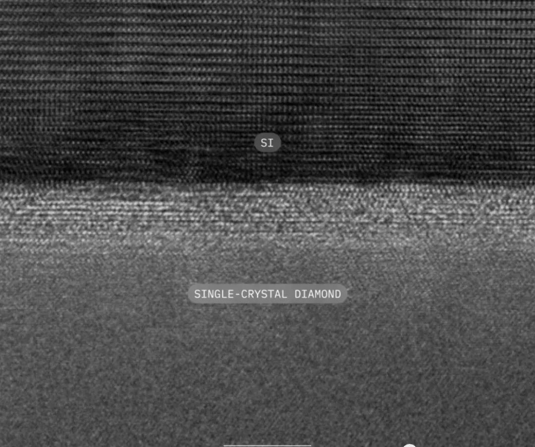
Currently, Diamond Foundry operates a diamond and wafer production facility in Washington State.It is reported that the company was established in 2012 and its business involves the jewelry and luxury goods markets as well as the semiconductor industry. The company said on its Linkedin website that it has received $515 million in financing and is executing a multi-billion dollar expansion plan to use zero-emission energy to convert greenhouse gases into diamond Si sheets.According to them, the company was able to achieve the ultimate thermal chip packaging by atomically bonding diamond to integrated circuit (IC) wafers thinned with angstrom-level precision.
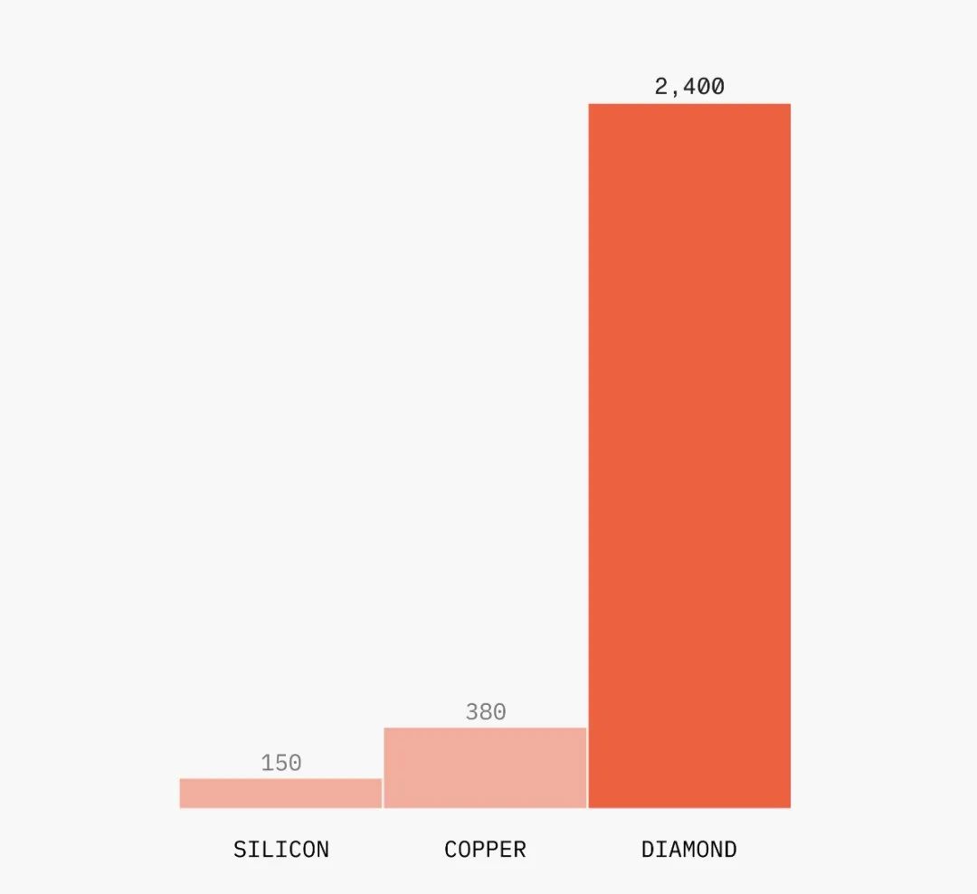
In terms of thermal conductivity, no other material conducts heat as effectively as single crystal diamond, allowing chips to run faster and last longer. This allows the diamond wafer to provide a thermal highway within atomic distance of the working chip's transistors. It dissipates heat with ideal efficiency, reducing hot spots and making the chip three times faster.
At the same time, it is an extreme electrical insulator, and the thinnest diamond slices can isolate very high voltages, allowing a new level of miniaturization of power electronics.
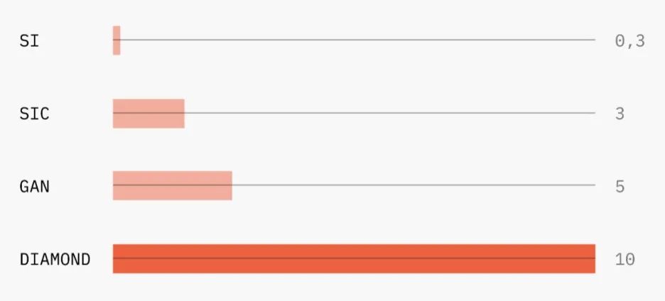
Thanks to these leading characteristics, Diamond Foundry believes that the company's solutions are suitable for all leading high-power chips. The combination of proven silicon chips with diamond semiconductor substrates greatly accelerates cloud and artificial intelligence computing, which means using data centers can get the same performance in half the space.
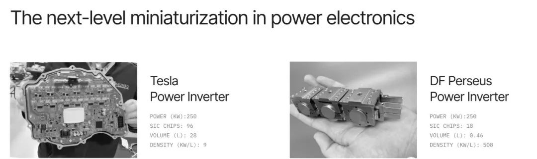
These advantages also allow it to simplify inverter design, because the extreme properties of the thermal conductivity and electrical insulation of diamond wafers enable the novel architecture to fundamentally advance miniaturization and improve efficiency. This leading design also allows it to help in the field of wireless communications.

According to reports, GaN semiconductors are powering a growing number of the most efficient wireless communications. But diamond wafers solve the overheating and voltage issues, making GaN better than SiC in every metric. The power density of diamond-based GaN MOSFETs is three times that of diamond-free GaN. Reliability is improved by reducing thermal stress and interconnecting GaN atoms to DF (Diamond Foundry) single crystal diamond.
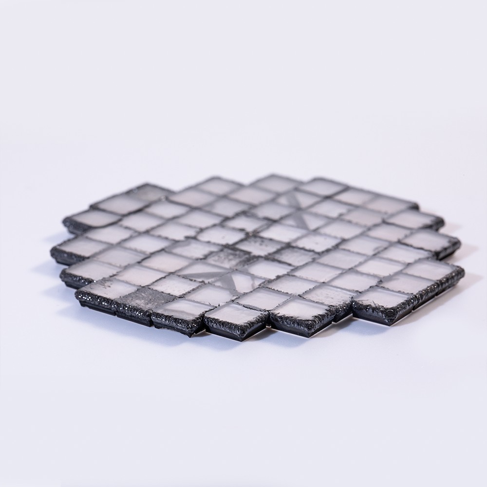
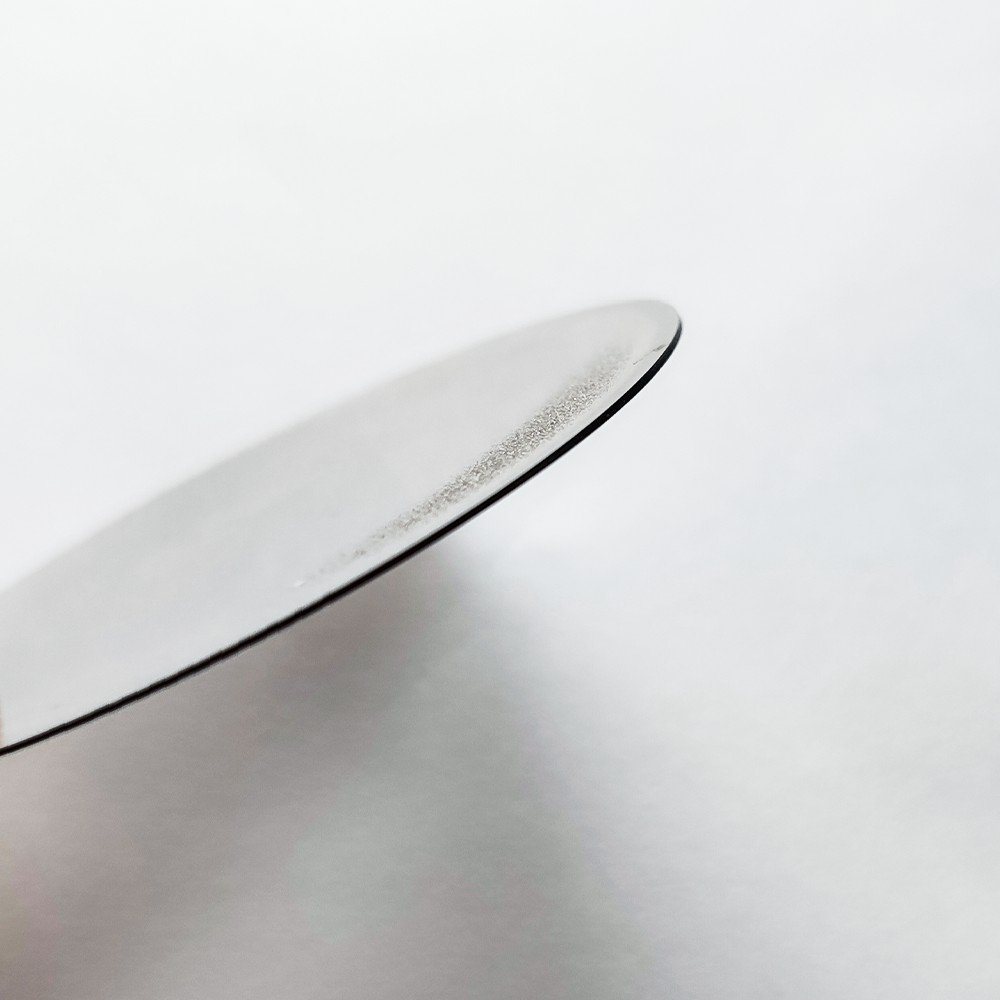
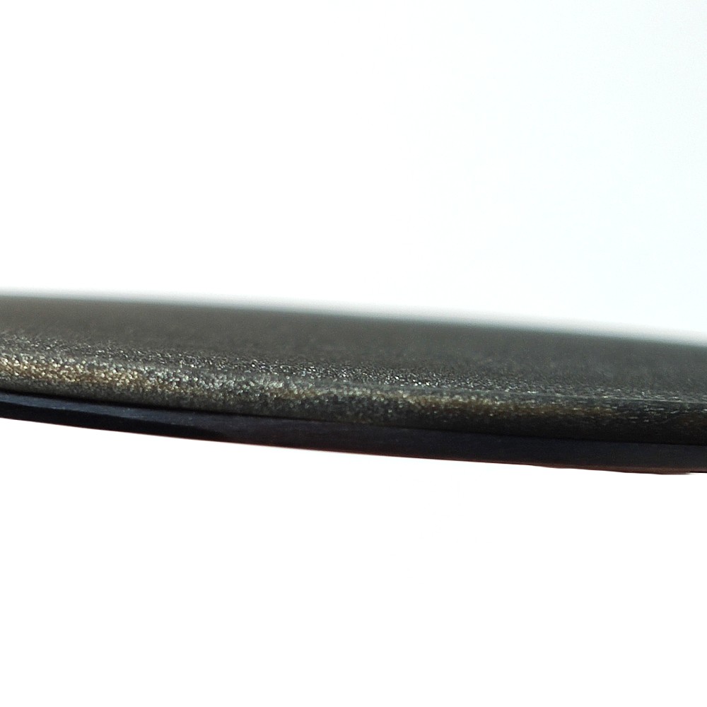
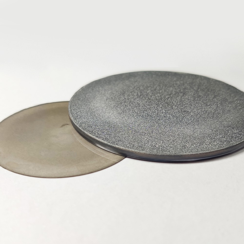
As a semiconductor diamond production supplier, High Light Intelligence Technology is developing rapidly in the semiconductor industry. We also provide diamond materials to major commercial customers and academic researchers, contributing to the development of semiconductor technology and materials.With MPCVD technology as the core, we have long been committed to the R&D and manufacturing of high-quality diamond materials and related equipment. We have advanced MPCVD equipment, laser processing equipment and precision polishing equipment.









-

CVD Single-Crystal Diamonds: An Analysis of the Complete Processing Workflow from Gas-Phase Deposition to Finished Diamond Chips
MPCVD (Microwave Plasma Chemical Vapor Deposition) technology is currently the core process for producing high-quality single-crystal diamond s. Thanks to its advantages of low defect rates, high purity, and controllable large dimensions, it is widely used in fields such as semiconductor heat dissipation, precision optics, and high-end sensors. The final quality of single-crystal diamond s depends on comprehensive process control throughout the entire workflow—from vapor deposition growth to pos
-
Single-Crystal or Polycrystalline Diamond — Which Has Greater Potential?
As diamond continues to enter industries such as semiconductors, thermal management, optics, high-power electronics, and precision machining, the requirements for diamond materials are also evolving.
-
Diamond Polishing and Grinding Processes: Core Challenges and Industry Hurdles
Diamond is often hailed as the “ultimate material” – ranking 10 on the Mohs hardness scale, boasting an ultra‑high thermal conductivity (~2,200 W/(m·K)), excellent chemical stability, and broad optical transparency. These properties make it irreplaceable in cutting‑edge applications such as semiconductor heat dissipation, high‑end optics, and quantum chips. Yet the paradox of “good materials are hard to process” is nowhere more evident than in diamond. From rough grinding for planarization to at
-
Single-Crystal vs Polycrystalline CVD Diamond: Process Difference Lies in Growth Logic, Not Equipment
The process difference between single crystal and polycrystalline CVD diamond lies not in equipment, but in growth logic. Single crystal and polycrystalline CVD diamond are two functional new materials with completely independent growth mechanisms, lattice structures and performance systems. Their process logic, product features and application boundaries diverge fundamentally from the very start of deposition and growth. Comparing or selecting materials without considering their underlying crys




