

- 中文
- English
- Español
High-quality diamond material preparation and electronic applications
2023-12-20 10:35:56
Click:
“
Diamond, because of its unique physical and chemical properties, has broad application prospects in many fields. Especially in the field of electronics, diamond's high thermal conductivity and high electron saturation mobility make it an ideal material for manufacturing high-performance electronic devices. However, there are still many challenges in preparing high-quality diamond materials and realizing their applications in the field of electronics. This article will explore the preparation met
”
Diamond, because of its unique physical and chemical properties, has broad application prospects in many fields. Especially in the field of electronics, diamond's high thermal conductivity and high electron saturation mobility make it an ideal material for manufacturing high-performance electronic devices. However, there are still many challenges in preparing high-quality diamond materials and realizing their applications in the field of electronics. This article will explore the preparation methods of high-quality diamond materials and their applications in the field of electronics.
Preparation of high-quality diamond materials: chemical vapor deposition (CVD)
Chemical vapor deposition is one of the main methods for preparing high-quality diamond materials. By controlling reaction conditions, such as temperature, pressure, gas composition, etc., high-quality, large-area diamond films can be synthesized. In addition, the CVD method can also achieve precise control of the composition and properties of diamond materials by changing the reaction precursors and dopants.
Applications of diamond in electronics:
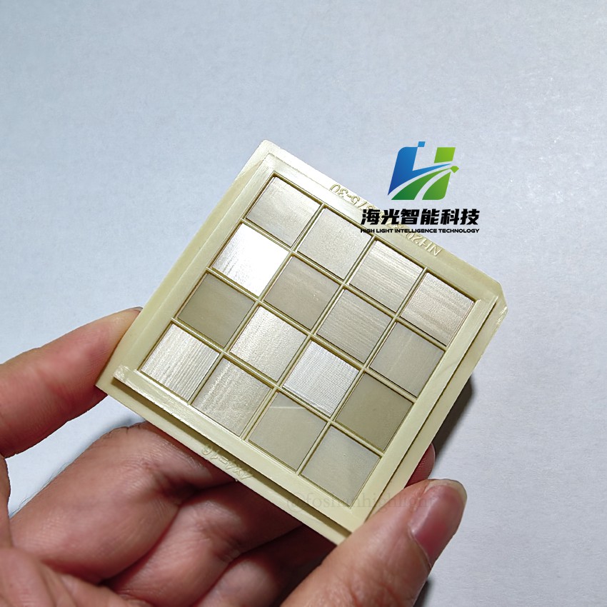
High-temperature electronic devices: Diamond’s high thermal conductivity and electrical insulation properties make it an ideal material for manufacturing high-temperature electronic devices. For example, diamond-based Schottky diodes have excellent performance in high-temperature environments and are expected to be used in energy conversion and sensing technologies in high-temperature environments.
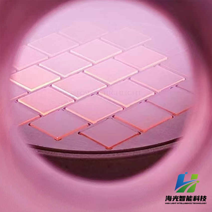
Deep ultraviolet optoelectronic devices: Diamond has a large band gap and is an ideal material for manufacturing deep ultraviolet optoelectronic devices. Deep ultraviolet light detectors prepared using diamond have broad application prospects in biomedicine, environmental monitoring and other fields.
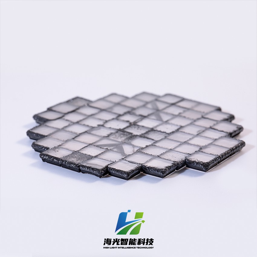
Nanoelectronic devices: Diamond’s large band gap and excellent mechanical, thermal, and chemical stability make it an ideal candidate material for fabricating nanoelectronic devices. For example, carbon nanotube field-effect transistors made of diamond show excellent performance in terms of low power consumption and high performance, and are expected to be used in the next generation of nanoelectronic devices.
The impact of MPCVD equipment on electronic applications:
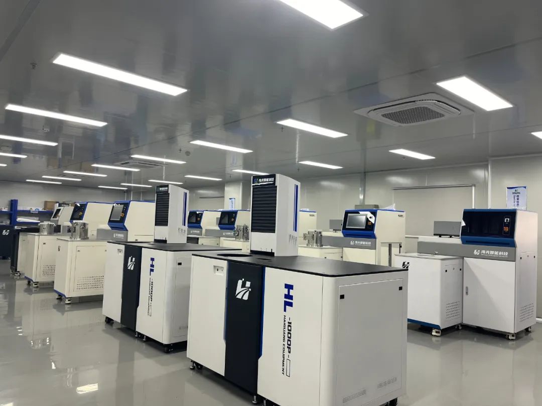
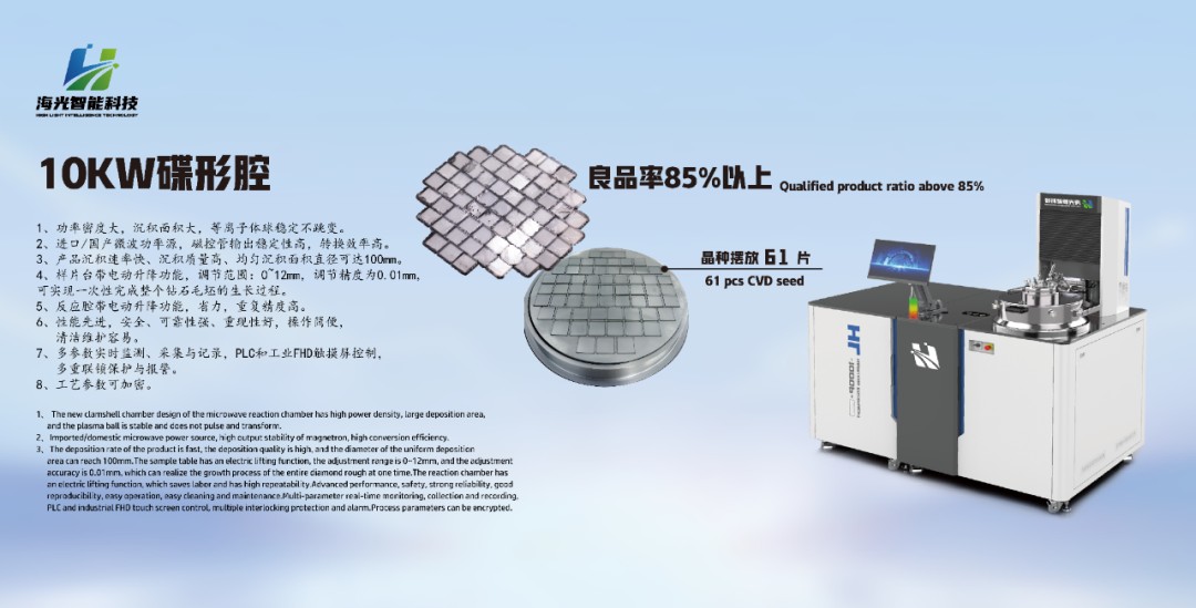
As an advanced diamond preparation technology, MPCVD equipment has had a profound impact on the field of electronics. First, MPCVD equipment enables the deposition of high-purity diamond films, which is crucial for manufacturing high-performance electronic devices. High-purity diamond films have excellent physical and chemical properties and can improve the performance and stability of electronic devices. Secondly, the deposition rate of MPCVD equipment can be increased by adjusting the microwave power, which greatly shortens the preparation cycle and improves production efficiency. This has important implications for mass production of electronic devices. In addition, MPCVD equipment can also achieve the preparation of large-area diamond films, which is of great significance for the manufacture of large-area, high-performance electronic devices. Finally, MPCVD equipment, as an advanced diamond preparation technology, provides new possibilities for the development of the electronics field. By continuously optimizing equipment performance and improving material quality, it is expected to realize the widespread application of diamond in the field of electronics and promote technological progress and innovative development in related fields.
Future outlook:
The preparation of high-quality diamond materials and their application in the field of electronics are hot and difficult topics in current research. By continuously optimizing preparation methods and improving material quality, it is expected to realize the widespread application of diamond in the field of electronics and promote technological progress and innovative development in related fields. At the same time, with the continuous advancement of science and technology and the introduction of innovative methods, it is believed that the application prospects of diamond in the field of electronics will be broader.









-

CVD Single-Crystal Diamonds: An Analysis of the Complete Processing Workflow from Gas-Phase Deposition to Finished Diamond Chips
MPCVD (Microwave Plasma Chemical Vapor Deposition) technology is currently the core process for producing high-quality single-crystal diamond s. Thanks to its advantages of low defect rates, high purity, and controllable large dimensions, it is widely used in fields such as semiconductor heat dissipation, precision optics, and high-end sensors. The final quality of single-crystal diamond s depends on comprehensive process control throughout the entire workflow—from vapor deposition growth to pos
-
Single-Crystal or Polycrystalline Diamond — Which Has Greater Potential?
As diamond continues to enter industries such as semiconductors, thermal management, optics, high-power electronics, and precision machining, the requirements for diamond materials are also evolving.
-
Diamond Polishing and Grinding Processes: Core Challenges and Industry Hurdles
Diamond is often hailed as the “ultimate material” – ranking 10 on the Mohs hardness scale, boasting an ultra‑high thermal conductivity (~2,200 W/(m·K)), excellent chemical stability, and broad optical transparency. These properties make it irreplaceable in cutting‑edge applications such as semiconductor heat dissipation, high‑end optics, and quantum chips. Yet the paradox of “good materials are hard to process” is nowhere more evident than in diamond. From rough grinding for planarization to at
-
Single-Crystal vs Polycrystalline CVD Diamond: Process Difference Lies in Growth Logic, Not Equipment
The process difference between single crystal and polycrystalline CVD diamond lies not in equipment, but in growth logic. Single crystal and polycrystalline CVD diamond are two functional new materials with completely independent growth mechanisms, lattice structures and performance systems. Their process logic, product features and application boundaries diverge fundamentally from the very start of deposition and growth. Comparing or selecting materials without considering their underlying crys




