

- 中文
- English
- Español
Japanese team releases diamond MOSFET to promote the popularization and practical application of diamond semiconductors
2024-01-12 10:45:58
Click:
“
Waseda University and Power Diamonds Systems (PDS) developed a structure in which the diamond surface is covered with silicon oxide terminations (C-Si-O terminations) that turn off the transistor when the gate voltage is 0V. To this end they announced the development of a "normally off" diamond MOSFET.
”
Waseda University and Power Diamonds Systems (PDS) developed a structure in which the diamond surface is covered with silicon oxide terminations (C-Si-O terminations) that turn off the transistor when the gate voltage is 0V. To this end they announced the development of a "normally off" diamond MOSFET.

The results were contributed by Professor Hiroshi Kawarada, FU Yu, Norito Narita, Xiahua Zhu, Waseda University Adjunct Professor Atsushi Hiraiwa, PDS's Kosuke Ota, PDS co-founder and CEO Tatsuya Fujishima and others. Details were announced on December 13 at IEEE International Electron Devices Meeting (IEDM 2023), an international conference on semiconductor device/process technology.
MOSFET
MOSFET is a field effect transistor (FET) with a MOS structure. It has the characteristics of high speed, low on-resistance, and high breakdown voltage. It is especially suitable as a switching element for motor driving. High-speed switching of large currents has been completed.
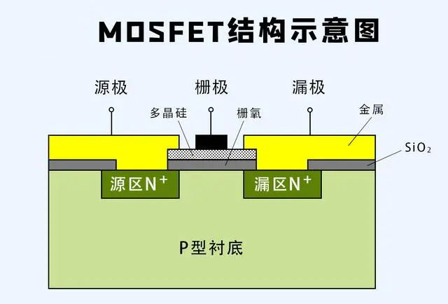
Therefore, if a normally-on device is applied to a power electronic device, there is no way to safely stop the device when it stops functioning normally, so normally-off operation is required. Against this background, the PDS and Waseda University research teams found that due to high-temperature oxidation, the C-H bonds of hydrogen atoms covering the diamond surface are transformed into CO bonds, and the surface becomes an electron defect, causing its performance to deteriorate. The company has been working on improving this to achieve stable operation of FETs.
In this study, we adopted a device structure in which the diamond surface has silicon oxide (C-Si-O) bonds instead of the traditional CO-Si bonds. As a result, the hole mobility of p-channel MOSFET is 150cm2/V·s, which is higher than the electron channel mobility of SiC n-channel MOSFET, and the signal threshold voltage of normally-off operation is 3~5V, which is the traditional diamond semiconductor Unachievable, a value said to prevent accidental conduction (short circuit).
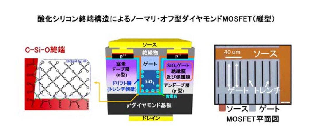
In addition, the maximum drain current of PDS for horizontal silicon oxide terminated diamond MOSFET exceeds 300 mA/mm, and the maximum drain current of vertical silicon oxide terminated diamond MOSFET exceeds 200 mA/mm. This is said to be the highest value for a normally-off diamond MOSFET in the series.
Both companies claim that by covering their surfaces with C-Si-O bonds, they have become stable devices that are more resistant to high temperatures and oxidation than traditional CH surfaces, and the company believes that their usability makes them suitable for mass production. To this end, Professor Kawaharada believes that diamond power semiconductors that are easy to implement in society have been realized, and PDS will continue to strengthen the research and development of diamond MOSFETs in order to popularize and practicalize diamond semiconductors. Their goal is to develop a device process suitable for mass production and achieve higher voltage resistance with a simpler structure.
High Light Intelligence Technology









-

CVD Single-Crystal Diamonds: An Analysis of the Complete Processing Workflow from Gas-Phase Deposition to Finished Diamond Chips
MPCVD (Microwave Plasma Chemical Vapor Deposition) technology is currently the core process for producing high-quality single-crystal diamond s. Thanks to its advantages of low defect rates, high purity, and controllable large dimensions, it is widely used in fields such as semiconductor heat dissipation, precision optics, and high-end sensors. The final quality of single-crystal diamond s depends on comprehensive process control throughout the entire workflow—from vapor deposition growth to pos
-
Single-Crystal or Polycrystalline Diamond — Which Has Greater Potential?
As diamond continues to enter industries such as semiconductors, thermal management, optics, high-power electronics, and precision machining, the requirements for diamond materials are also evolving.
-
Diamond Polishing and Grinding Processes: Core Challenges and Industry Hurdles
Diamond is often hailed as the “ultimate material” – ranking 10 on the Mohs hardness scale, boasting an ultra‑high thermal conductivity (~2,200 W/(m·K)), excellent chemical stability, and broad optical transparency. These properties make it irreplaceable in cutting‑edge applications such as semiconductor heat dissipation, high‑end optics, and quantum chips. Yet the paradox of “good materials are hard to process” is nowhere more evident than in diamond. From rough grinding for planarization to at
-
Single-Crystal vs Polycrystalline CVD Diamond: Process Difference Lies in Growth Logic, Not Equipment
The process difference between single crystal and polycrystalline CVD diamond lies not in equipment, but in growth logic. Single crystal and polycrystalline CVD diamond are two functional new materials with completely independent growth mechanisms, lattice structures and performance systems. Their process logic, product features and application boundaries diverge fundamentally from the very start of deposition and growth. Comparing or selecting materials without considering their underlying crys




