

- 中文
- English
- Español
Xi'an Jiaotong University achieves mass production of 2-inch heteroepitaxial single crystal diamond substrate
2024-01-26 09:13:15
Click:
“
Compared with traditional silicon materials, wide bandgap semiconductor materials are more suitable for making high-voltage, high-frequency, and high-power semiconductor devices, and are considered to be a key player in material innovation in the post-Moore era. Single crystal diamond has excellent properties such as large band gap, high thermal conductivity, and high mobility, and is an ideal semiconductor material for the next generation of high-power and high-frequency electronic devices. How
”
Recently, the Xi'an Jiaotong University research team used microwave plasma chemical vapor deposition (MPCVD) technology to successfully achieve batch production of 2-inch heteroepitaxial single crystal diamond self-supporting substrates (as shown in the picture above). Through effective control of film formation uniformity, temperature field and flow field, the yield of heteroepitaxial single crystal diamond is improved. The substrate surface has a step-flow growth mode (as shown in the figure below), which can reduce the defect density of the substrate and improve the crystal quality. The half-peak widths of XRD (004) and (311) rocking curves are less than 91 arcsec and 111 arcsec respectively (as shown in the figure below), reaching the world's leading level.
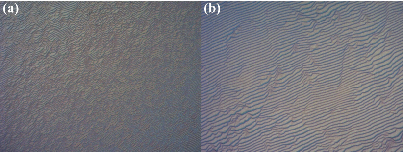
Figure: Optical microscope photo of heteroepitaxial diamond (a) magnified 100 times (b) magnified 500 times
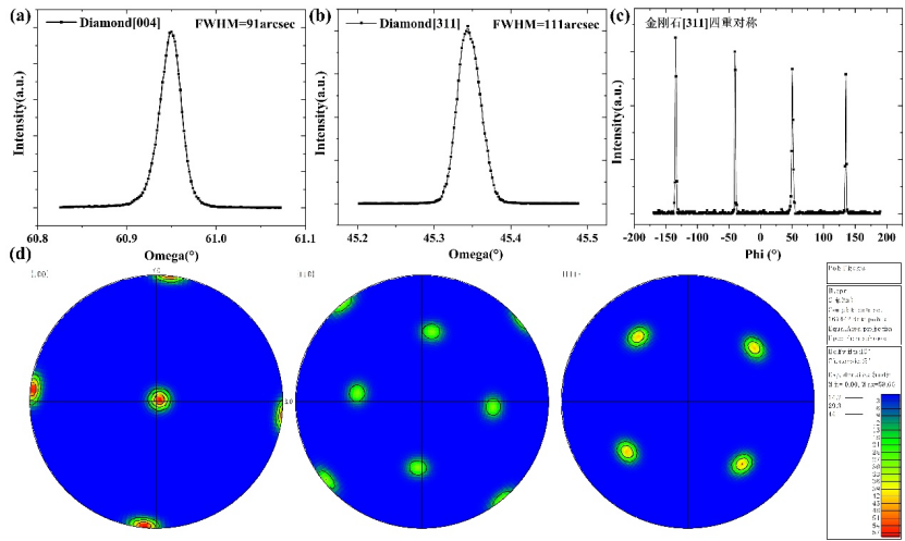
Figure: XRD test results (a) (004) surface rocking curve; (b) (311) surface rocking curve; (c) (311) surface four-fold symmetry; (d) pole figure
This method uses microwave plasma to excite reactive gases to achieve the growth of heteroepitaxial single crystal diamond at lower temperatures and pressures. Compared with traditional preparation methods, this method has higher growth rate and lower cost, while enabling large-scale production. This will effectively ensure the demand for high-quality, large-size electronic-grade single crystal diamond in domestic power electronic devices, thermal conductivity, radar detection and other fields, while also meeting the demand for high-quality seed crystals for scientific research in colleges and universities.
It is worth mentioning that the industrialization of this research results has broken the foreign technology monopoly, reduced the production costs of related domestic industries, and has broad application prospects. With the rapid development of emerging technologies such as 5G and the Internet of Things, the demand for diamond applications in electronics, photonics, quantum and other fields continues to increase. The mass production of heteroepitaxial single crystal diamond substrates will provide more stable and reliable raw material support for the development of related industries. At the same time, the promotion and application of this achievement will also drive the development of related industrial chains and promote the transformation and upgrading of our country's economy. We look forward to more applications and breakthroughs of this technology in the future.
Xi'an Jiaotong University's Wide Bandgap Semiconductor Materials and Devices Research Center was established in 2013. The director of the laboratory is Professor Wang Hongxing, a nationally appointed expert. After nearly 10 years of development, the laboratory has formed a series of technologies such as diamond semiconductor epitaxial equipment research and development, single crystal/polycrystalline substrate growth, and electronic device development with independent intellectual property rights, and has been authorized 48 patents. Extensive cooperation on diamond semiconductor materials and devices has been carried out with relevant large domestic communication companies, relevant research institutes of China Electronics Technology, etc., which has promoted the practical development of diamond radio frequency power electronic devices, power electronic devices, MEMS and other devices.
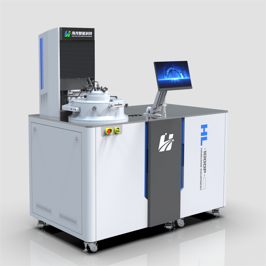
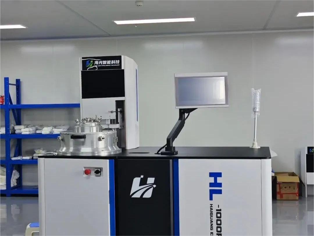
High Light Intelligence Technology, as a semiconductor diamond production supplier, while the semiconductor industry is developing rapidly, we also provide diamond materials to major commercial customers and academic researchers, contributing to the development of semiconductor technology and materials. With MPCVD technology as the core, we have long been committed to the R&D and manufacturing of high-quality diamond materials and related equipment. We have advanced MPCVD equipment, laser processing equipment and precision polishing equipment.









-

CVD Single-Crystal Diamonds: An Analysis of the Complete Processing Workflow from Gas-Phase Deposition to Finished Diamond Chips
MPCVD (Microwave Plasma Chemical Vapor Deposition) technology is currently the core process for producing high-quality single-crystal diamond s. Thanks to its advantages of low defect rates, high purity, and controllable large dimensions, it is widely used in fields such as semiconductor heat dissipation, precision optics, and high-end sensors. The final quality of single-crystal diamond s depends on comprehensive process control throughout the entire workflow—from vapor deposition growth to pos
-
Single-Crystal or Polycrystalline Diamond — Which Has Greater Potential?
As diamond continues to enter industries such as semiconductors, thermal management, optics, high-power electronics, and precision machining, the requirements for diamond materials are also evolving.
-
Diamond Polishing and Grinding Processes: Core Challenges and Industry Hurdles
Diamond is often hailed as the “ultimate material” – ranking 10 on the Mohs hardness scale, boasting an ultra‑high thermal conductivity (~2,200 W/(m·K)), excellent chemical stability, and broad optical transparency. These properties make it irreplaceable in cutting‑edge applications such as semiconductor heat dissipation, high‑end optics, and quantum chips. Yet the paradox of “good materials are hard to process” is nowhere more evident than in diamond. From rough grinding for planarization to at
-
Single-Crystal vs Polycrystalline CVD Diamond: Process Difference Lies in Growth Logic, Not Equipment
The process difference between single crystal and polycrystalline CVD diamond lies not in equipment, but in growth logic. Single crystal and polycrystalline CVD diamond are two functional new materials with completely independent growth mechanisms, lattice structures and performance systems. Their process logic, product features and application boundaries diverge fundamentally from the very start of deposition and growth. Comparing or selecting materials without considering their underlying crys




