

- 中文
- English
- Español
Russian researchers successfully prepare stable graphene-diamond nanocomposite
2024-05-08 09:44:31
Click:
“
Diamonds have long been of great significance in basic science and technology. Their excellent mechanical properties, high thermal conductivity, wide bandgap, optical properties, biocompatibility and potential for quantum applications make them exceptional.
”
Diamond has long occupied a core position in basic science and technology, and its outstanding mechanical properties, high thermal conductivity, wide bandgap, optical properties, biocompatibility and quantum potential are all impressive. With its unique properties, nanodiamond has shown great technological potential in the fields of electronics, optics and biomedicine, and has attracted widespread attention. However, its stability is still a difficult problem to be solved. Compared to graphite, diamond is less stable and is only protected by kinetic barriers. Nanoscale diamond surface effects may weaken this protection, threatening overall structural stability. Even in a stable state, nanodiamond structures face challenges under harsh conditions during the synthesis process.

Multilayer graphene serves as an irradiation target, providing a new way to create specific ultrathin diamond films. Its high surface ratio allows graphene drilling to be achieved locally across the thickness of the film, providing opportunities for modulating electronic properties. For example, electron irradiation can locally form bonds between graphene layers, forming carrier barriers. Rapid heavy ion irradiation of multilayer graphene (located on a SiO2 substrate) can form pores or local structural damping, affecting conductivity. Among them, the formation of single-crystal two-dimensional nanodiamond (two-dimensional diamond) during the irradiation process is of particular concern. Rapid heavy ion irradiation with MeV energy shows the potential to form diamond, which is achieved through sharp heating and shock waves, and can form a two-dimensional diamond film like a (100) surface without affecting surface graphitization.
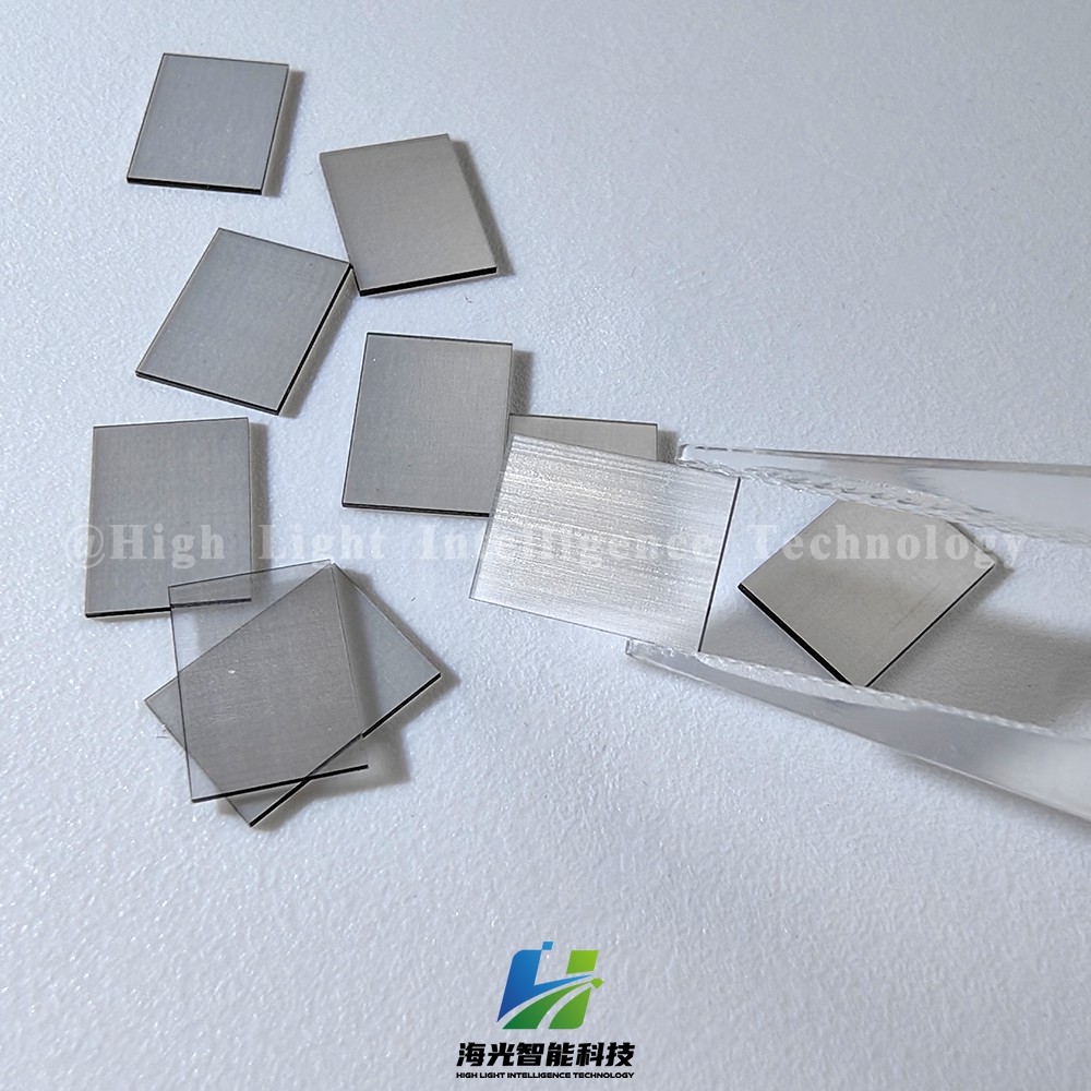
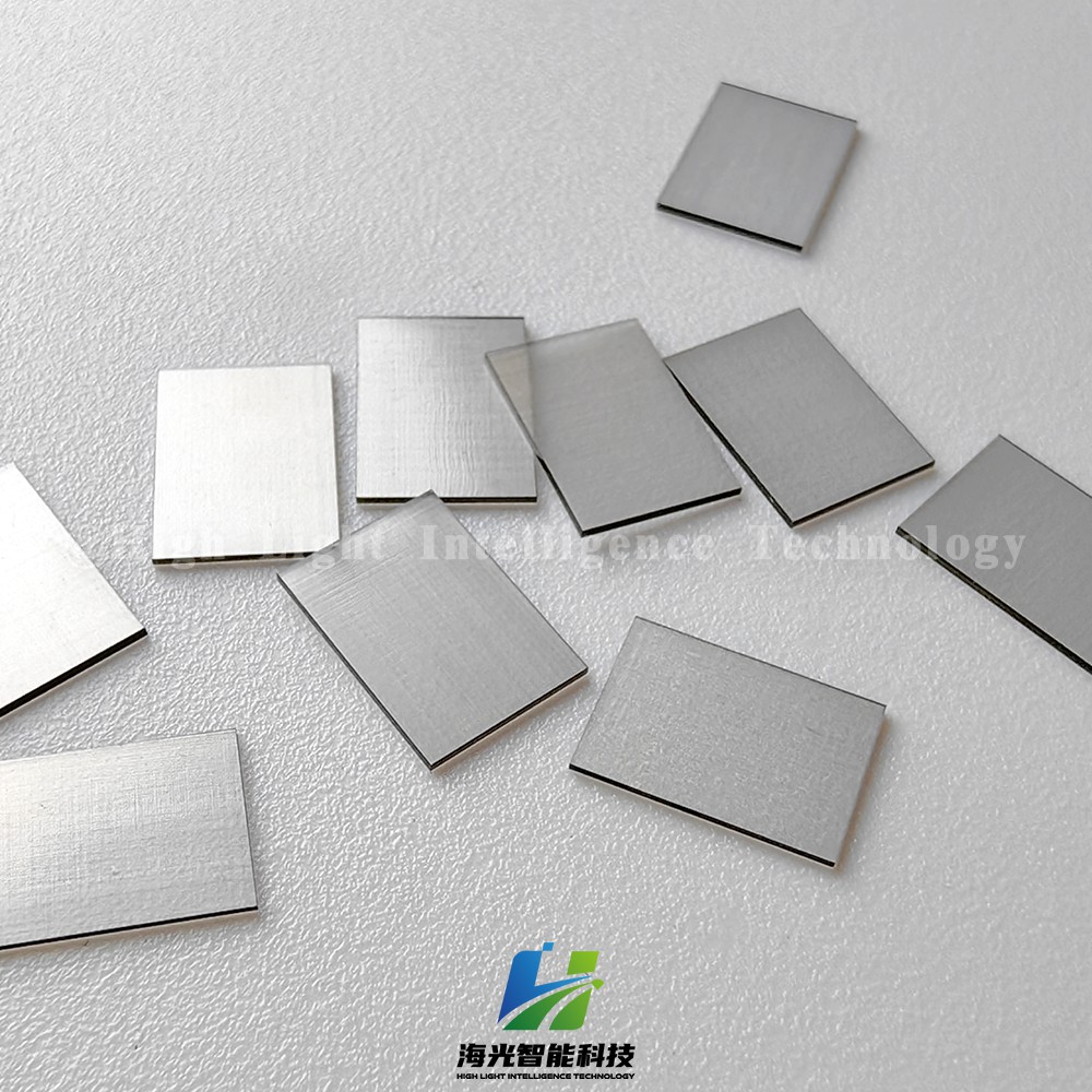
Researchers from the Moscow Institute of Steel and Alloys, the Institute of Semiconductor Physics of the Siberian Branch and the Dubna Joint Institute for Nuclear Research successfully prepared stable graphene-diamond nanostructure composite materials by bombarding multi-layer graphene with high-energy heavy ions. This new material is lightweight and combines the conductivity of graphene with the hardness of diamond, bringing huge potential for fields such as aerospace and biomedical devices. The study has verified for the first time that Xe26+ ions can form 5 to 20 nanometer nanodiamonds and two-dimensional diamond clusters in graphene at energies of 26 to 167 MeV. The relevant results have been published in "Carbon".
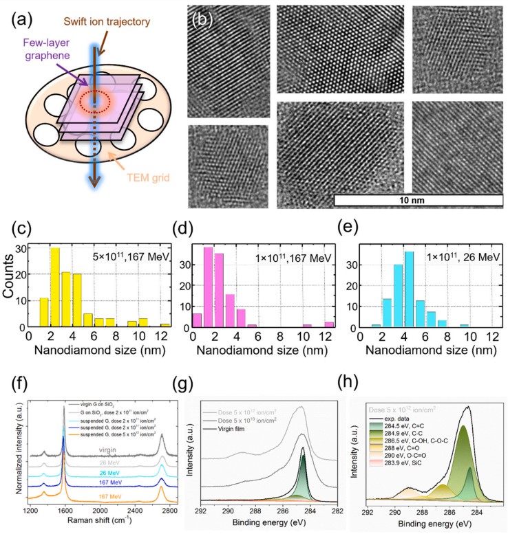
Figure 1. a) Sketch of sample irradiated with high-energy Xe ions. b) High-resolution transmission electron microscopy image of nanosized diamonds embedded in few-layer graphene films. c-e) Nanodiamond size distribution. f) Raman spectra of unirradiated and irradiated FLG films. g,h) XPS spectrum of CVD FLG film decomposed into components.
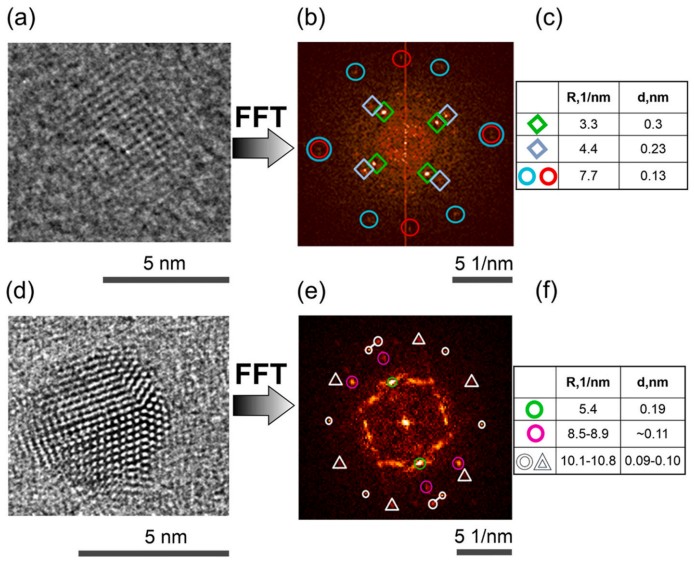
Figure 2. Magnified fragments of HRTEM images for CVD few-layer graphene films irradiated with 26 (a) and 167 (d) MeV Xe ions respectively; the corresponding fast Fourier transform (FFT) pattern is (b) and (e). Some bright spots, marked by colored circles and squares, are detailed in tables (c) and (f). The irradiation doses are 1×10¹¹ and 5×10¹¹ ions/cm² respectively.
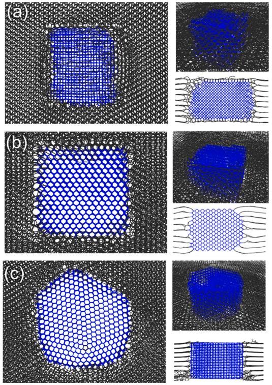
Figure 3. (a) Top, perspective and side views of 2D diamond embedded graphene with (100) plane. (b), (c) Top, perspective and side views of 2D diamond embedded in graphene with (110) plane. In (c), a diamond cluster containing pentagonal defects is presented. The sp² and sp³ bonds are represented by black and blue sticks, respectively.
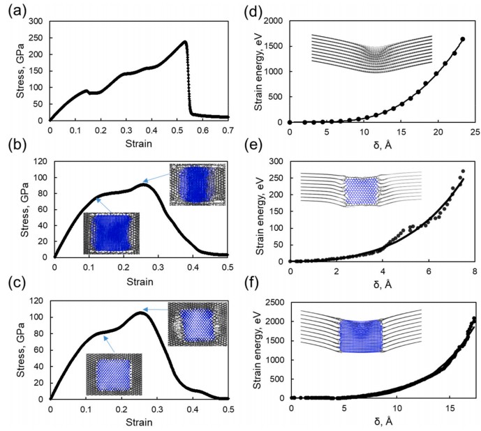
Figure 4. a-c) Mechanical properties of graphene-based films. Stress-strain curves of 9-layer graphene (a) and graphene-diamond (100) (b) and graphene-diamond (110) (c) hybrid structures. d-f) Indentation energy-deflection curves of 9-layer graphene (d) and graphene-diamond (100) (e) and graphene-diamond (110) (f) hybrid structures.
Researchers have successfully revealed the huge potential of irradiating graphene with fast heavy ions to generate two-dimensional diamond. In graphene films, the nanostructure exhibits a regular diamond structure, and its changes are regulated by ion dose and energy. By adjusting these parameters, clusters of various sizes consistent with theoretical predictions were experimentally obtained. It is worth noting that this method can uniquely prepare diamond films on the (110) and (100) surfaces, while other surfaces are prone to graphitization. The study also found that the thickness of the graphene film is crucial to the formation of the diamond structure. Films with less than six layers only produce (110) surface diamond clusters, while films with less than four layers cannot maintain the diamond structure. Evaluation of the mechanical stiffness of the composite (graphene/diamond) shows that although it is more brittle than pristine graphene, it is equally hard. Even when subjected to indentation, the stiffness of the cluster region significantly exceeds that of the pristine graphene film.
The fabrication of diamond structures in graphene provides a new way to tailor the properties of ultrathin diamond films, with potential in electronics, optics and biomedicine. Its stability and excellent performance make it a strong candidate for future technological innovation and is expected to play an important role in aerospace, automotive, medical and other fields.









-

CVD Single-Crystal Diamonds: An Analysis of the Complete Processing Workflow from Gas-Phase Deposition to Finished Diamond Chips
MPCVD (Microwave Plasma Chemical Vapor Deposition) technology is currently the core process for producing high-quality single-crystal diamond s. Thanks to its advantages of low defect rates, high purity, and controllable large dimensions, it is widely used in fields such as semiconductor heat dissipation, precision optics, and high-end sensors. The final quality of single-crystal diamond s depends on comprehensive process control throughout the entire workflow—from vapor deposition growth to pos
-
Single-Crystal or Polycrystalline Diamond — Which Has Greater Potential?
As diamond continues to enter industries such as semiconductors, thermal management, optics, high-power electronics, and precision machining, the requirements for diamond materials are also evolving.
-
Diamond Polishing and Grinding Processes: Core Challenges and Industry Hurdles
Diamond is often hailed as the “ultimate material” – ranking 10 on the Mohs hardness scale, boasting an ultra‑high thermal conductivity (~2,200 W/(m·K)), excellent chemical stability, and broad optical transparency. These properties make it irreplaceable in cutting‑edge applications such as semiconductor heat dissipation, high‑end optics, and quantum chips. Yet the paradox of “good materials are hard to process” is nowhere more evident than in diamond. From rough grinding for planarization to at
-
Single-Crystal vs Polycrystalline CVD Diamond: Process Difference Lies in Growth Logic, Not Equipment
The process difference between single crystal and polycrystalline CVD diamond lies not in equipment, but in growth logic. Single crystal and polycrystalline CVD diamond are two functional new materials with completely independent growth mechanisms, lattice structures and performance systems. Their process logic, product features and application boundaries diverge fundamentally from the very start of deposition and growth. Comparing or selecting materials without considering their underlying crys




