

- 中文
- English
- Español
Wide application of High Light Intelligence Technology's CVD diamond polycrystalline products
2024-07-19 09:50:57
Click:
“
In recent years, with the rapid development of science and technology, diamond, as a high-performance material, has shown great application potential in many fields. As a leader in the field of diamond material production and research and development, High Light Intelligence Technology has successfully launched CVD diamond polycrystalline wafer based on MPCVD technology through independent research and development and innovation. These products have been widely used in the market and have won w
”
In recent years, with the rapid development of science and technology, diamond, as a high-performance material, has shown great application potential in many fields. As a leader in the field of diamond material production and research and development, High Light Intelligence Technology has successfully launched CVD diamond polycrystalline wafer based on MPCVD technology through independent research and development and innovation. These products have been widely used in the market and have won wide recognition in the industry for their unique advantages and characteristics.
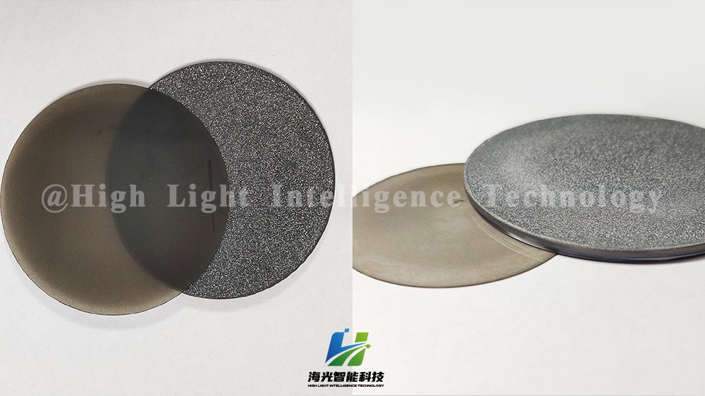
CVD diamond polycrystalline wafer are becoming increasingly important in high-tech and industrial fields due to their excellent performance and wide application. With technological progress and market growth, their application areas will continue to expand.
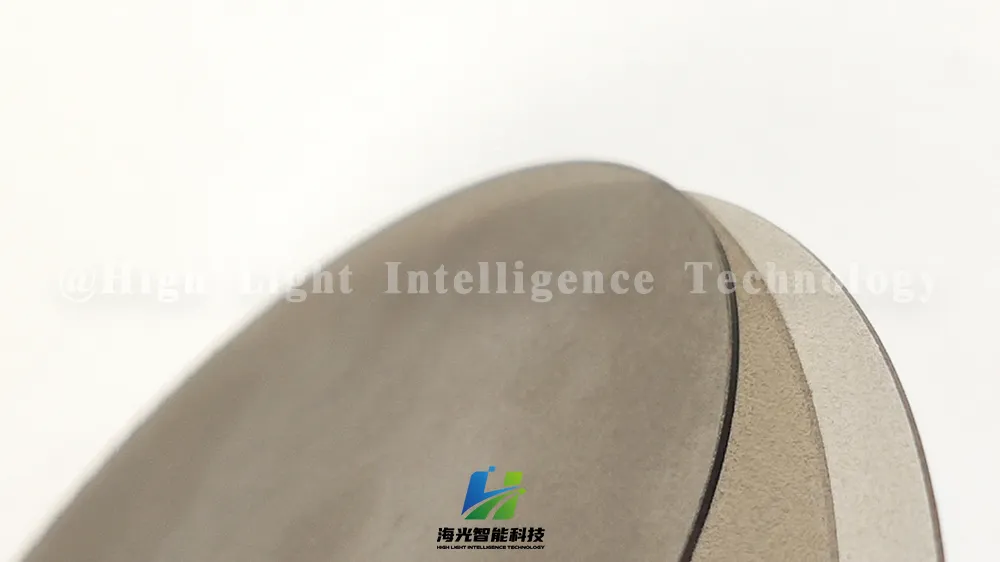
Advantage:
Excellent physical properties:
Top hardness, suitable for high-strength processing; extremely low thermal expansion coefficient, suitable for high-precision processing.
Excellent thermal conductivity:
The thermal conductivity is far higher than copper, which is the preferred material in the field of heat dissipation, ensuring stable operation of the equipment.
Wide-band high transmittance:
High transmittance from deep ultraviolet to far infrared, suitable for optical instruments and communication equipment.
Stable chemical properties:
Resistant to chemical corrosion, suitable for long-term use in harsh environments, stable and reliable performance.
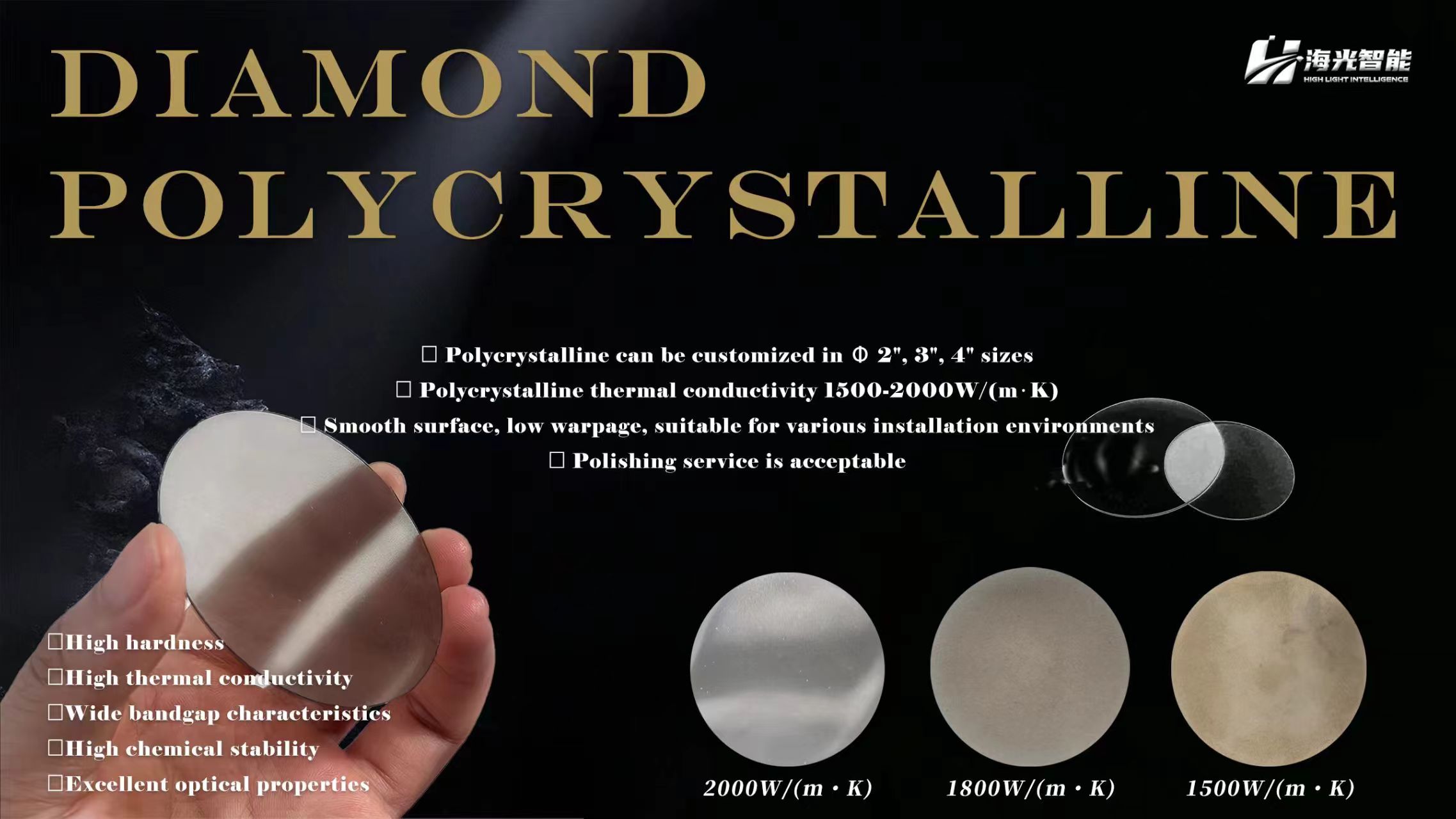
Widely Used:
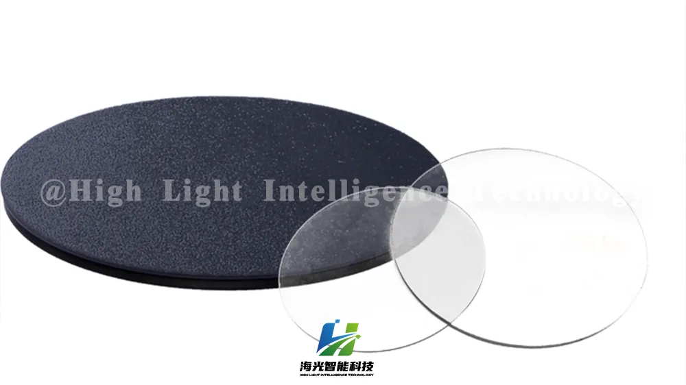
High-precision processing field
CVD diamond polycrystalline wafer have become an ideal choice in the field of high-precision processing due to their extremely high hardness and wear resistance. Whether it is wafer cutting in the semiconductor industry or precision parts processing in the aerospace field, diamond can provide excellent processing quality and efficiency.
Heat dissipation field
With the continuous development of electronic equipment, the problem of heat dissipation has become increasingly prominent. CVD diamond polycrystalline wafer have become a key material for solving heat dissipation problems with their excellent thermal conductivity. In applications such as CPU radiators and LED lamp heat sinks, diamond can quickly export heat to ensure the stable operation of the equipment.
Optical field
The wide-band high transmittance of CVD diamond polycrystalline wafer gives it a wide range of application prospects in the optical field. Whether it is the output window of a high-power laser or the protective window of an infrared detector, diamond can provide excellent optical performance to ensure the sensitivity and stability of the equipment.
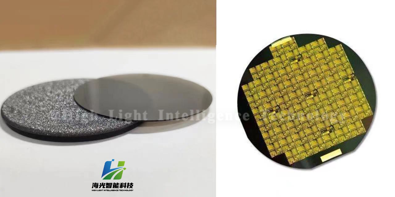
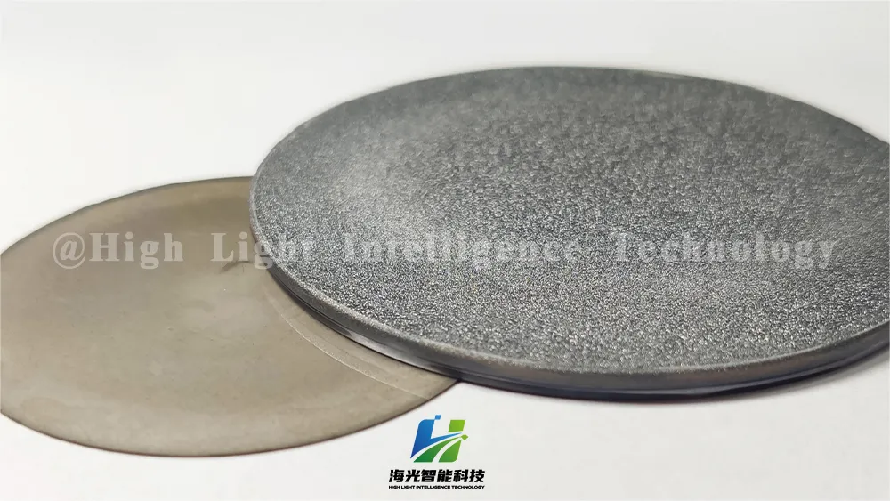
Through independent research and development and innovation, High Light Intelligence Technology has successfully launched diamond polycrystalline products based on MPCVD technology. These products have been widely used in many fields with their excellent physical properties, excellent thermal conductivity, wide-band high transmittance and stable chemical properties. In the future, with the continuous advancement of science and technology and the continuous expansion of the market, CVD diamond polycrystalline wafer will surely usher in a broader development prospect.









-

Foshan Highlight Intelligent Technology invites you to the 140th Canton Fair—join us at Booth 21.2A23-24 in the Friendship Hall to share in the brilliance.
Foshan Highlight Intelligent Technology invites you to the 140th Canton Fair—join us at Booth 21.2A23-24 in the Friendship Hall to share in the brilliance.
-
CVD Single-Crystal Diamonds: An Analysis of the Complete Processing Workflow from Gas-Phase Deposition to Finished Diamond Chips
MPCVD (Microwave Plasma Chemical Vapor Deposition) technology is currently the core process for producing high-quality single-crystal diamond s. Thanks to its advantages of low defect rates, high purity, and controllable large dimensions, it is widely used in fields such as semiconductor heat dissipation, precision optics, and high-end sensors. The final quality of single-crystal diamond s depends on comprehensive process control throughout the entire workflow—from vapor deposition growth to pos
-
Single-Crystal or Polycrystalline Diamond — Which Has Greater Potential?
As diamond continues to enter industries such as semiconductors, thermal management, optics, high-power electronics, and precision machining, the requirements for diamond materials are also evolving.
-
Diamond Polishing and Grinding Processes: Core Challenges and Industry Hurdles
Diamond is often hailed as the “ultimate material” – ranking 10 on the Mohs hardness scale, boasting an ultra‑high thermal conductivity (~2,200 W/(m·K)), excellent chemical stability, and broad optical transparency. These properties make it irreplaceable in cutting‑edge applications such as semiconductor heat dissipation, high‑end optics, and quantum chips. Yet the paradox of “good materials are hard to process” is nowhere more evident than in diamond. From rough grinding for planarization to at




