

- 中文
- English
- Español
Advantages of CVD single crystal diamond in industrial applications
2025-12-26 16:02:49
Click:
“
CVD (Chemical Vapor Deposition) single-crystal diamond, as an industrial application material, represents the forefront of cutting-edge materials science. It inherits almost all the excellent properties of natural diamond and achieves large-size, high-quality, and customizable production through artificial methods. Its core advantage lies in its combination of multiple extreme properties, which is unmatched by other materials.
”
CVD (Chemical Vapor Deposition) single-crystal diamond, as an industrial application material, represents the forefront of cutting-edge materials science. It inherits almost all the excellent properties of natural diamond and achieves large-size, high-quality, and customizable production through artificial methods. Its core advantage lies in its combination of multiple extreme properties, which is unmatched by other materials.
1
Unparalleled Thermal Conductivity:
Value: 2000-2200 W/(m·K) at room temperature, 5 times that of copper (approximately 400 W/(m·K)) and more than 10 times that of commonly used packaging materials such as aluminum nitride (AlN).
Industrial Value: This is one of its most notable advantages. It can rapidly dissipate heat from heat sources (such as high-power laser chips, microwave devices, and CPU cores), greatly reducing device junction temperature and improving performance, reliability, and lifespan.

2
Extremely High Hardness and Wear Resistance
With a Mohs hardness of 10, it is the hardest known substance.
Industrial Value: An ideal material for ultra-precision machining tools (such as cutting tools and dressing pens), wear-resistant components, and high-performance bearings, with a service life far exceeding that of traditional materials like cemented carbide and alumina.
3
Extremely Wide Optical Transmission Window
It exhibits high transmittance from deep ultraviolet (225 nm) to far-infrared (microwave band), and is non-hygroscopic and susceptible to acid and alkali corrosion.
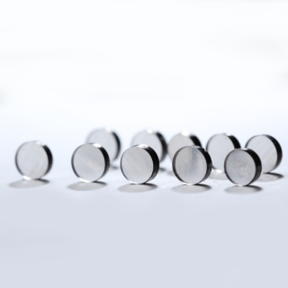
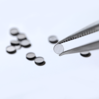
Industrial Value: It is the ultimate material for manufacturing optical devices for extreme environments such as output windows of high-power lasers, missile fairings, and synchrotron X-ray windows. It can withstand high-energy laser beams without thermal lensing effects, or maintain optical performance under high-speed, high-temperature, and rain-erosion environments.
4
Extremely High Breakdown Electric Field and Excellent Electrical Properties
The breakdown electric field reaches 10 MV/cm, tens of times that of silicon. It also possesses very high carrier mobility (both electron and hole mobility are high).
Fourth-Generation Semiconductor Material Suitable for high-voltage, high-power, high-frequency, and high-temperature electronic devices (such as power diodes and field-effect transistors), its theoretical performance far surpasses that of silicon carbide (SiC) and gallium nitride (GaN), significantly reducing power conversion losses.
5
Extremely low coefficient of friction and chemical inertness
It has an extremely low coefficient of friction and exhibits extremely high resistance to acidic, alkaline, and high-temperature environments.
Industrial value: Used in mechanical sealing rings and biocompatible coatings in special environments. In corrosive media, its sealing performance and service life far exceed those of traditional materials.
Thermal Management (“Ultimate Heat Sink”): High-power laser diodes (pump sources), 5G/6G RF devices, and heat dissipation substrates for power electronic modules (IGBT, GaN). Rapid heat dissipation is key to solving the “thermal barrier” problem in next-generation electronic devices.
Precision/Ultra-Precision Machining: Ultra-precision cutting tools (machining non-ferrous metals and composite materials), grinding wheel dressing pens, and wire drawing dies. Their ultra-long lifespan and sharpness significantly improve machining accuracy and efficiency.
Optics: High-power CO2 laser windows, infrared military optical systems (radomes, windows), free-electron lasers and synchrotron radiation beamline windows, and Raman laser cavities. Maintaining optical performance under extreme conditions.
Other High-Tech Fields: Cutting-edge scientific instruments (such as high-pressure anvils), biosensors, and high-performance acoustic devices (hypersonic).
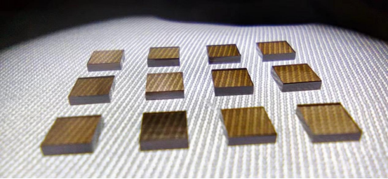
Foshan High Light's new machines can currently produce 500 carats of single-crystal diamonds per month, with jewelry-grade DEF color and VVS-VS clarity.
If semiconductor-grade heat sink single-crystal diamonds are grown, the output can be increased by 2-3 times from 500 carats.
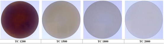
Polycrystalline wafers can be grown in sizes of 2', 3', and 4', with thermal conductivity reaching 1500 W/m·K, 1800 W/m·K, and 2000 W/m·K, respectively. Visible light transmittance can reach 67%-85%.
Optical-grade single crystal diamond, polycrystalline, and medical ophthalmic instruments can be customized. Please contact us and provide your product requirements and quantity.
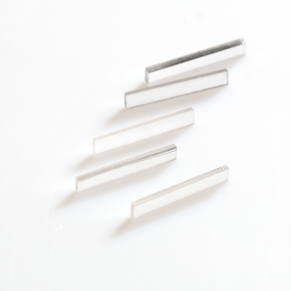
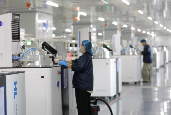
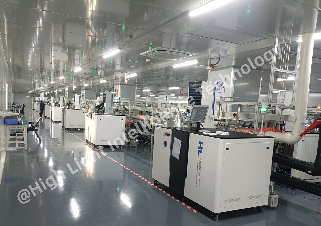
High Light Intelligence Technology, a pioneer in the CVD diamond industry, has advanced MPCVD technology and CVD diamond production workshops. We focus on producing high-purity lab-grown diamonds for the jewelry industry, and at the same time create industrial-grade CVD diamond products, covering single crystals, polycrystalline, films and diamond surface metallization. We also provide 6kw/10kw/15kw MPCVD equipment to help customers in all aspects, from equipment to products, and then to all-round services, to create brilliance together.









-

CVD Single-Crystal Diamonds: An Analysis of the Complete Processing Workflow from Gas-Phase Deposition to Finished Diamond Chips
MPCVD (Microwave Plasma Chemical Vapor Deposition) technology is currently the core process for producing high-quality single-crystal diamond s. Thanks to its advantages of low defect rates, high purity, and controllable large dimensions, it is widely used in fields such as semiconductor heat dissipation, precision optics, and high-end sensors. The final quality of single-crystal diamond s depends on comprehensive process control throughout the entire workflow—from vapor deposition growth to pos
-
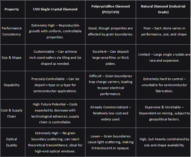
Single-Crystal or Polycrystalline Diamond — Which Has Greater Potential?
As diamond continues to enter industries such as semiconductors, thermal management, optics, high-power electronics, and precision machining, the requirements for diamond materials are also evolving.
-
Diamond Polishing and Grinding Processes: Core Challenges and Industry Hurdles
Diamond is often hailed as the “ultimate material” – ranking 10 on the Mohs hardness scale, boasting an ultra‑high thermal conductivity (~2,200 W/(m·K)), excellent chemical stability, and broad optical transparency. These properties make it irreplaceable in cutting‑edge applications such as semiconductor heat dissipation, high‑end optics, and quantum chips. Yet the paradox of “good materials are hard to process” is nowhere more evident than in diamond. From rough grinding for planarization to at
-
Single-Crystal vs Polycrystalline CVD Diamond: Process Difference Lies in Growth Logic, Not Equipment
The process difference between single crystal and polycrystalline CVD diamond lies not in equipment, but in growth logic. Single crystal and polycrystalline CVD diamond are two functional new materials with completely independent growth mechanisms, lattice structures and performance systems. Their process logic, product features and application boundaries diverge fundamentally from the very start of deposition and growth. Comparing or selecting materials without considering their underlying crys




