

- 中文
- English
- Español
The Metamorphosis of Diamond: From Jewelry to a Cornerstone of Technology—Three Key High-Tech Applications of CVD Single-Crystal Diamond Wafers
2026-08-14 15:41:28
Click:
“
When you hear the word "diamond," what comes to mind first? Is it dazzling diamond jewelry, or the romantic vow that "a diamond is forever"?
In reality, diamond is making a major breakthrough in the realms of industry and technology—demonstrating its value in a truly "hardcore" way. Thanks to its status as the hardest material in nature, its exceptional thermal conductivity, and its broad optical transparency (spanning from ultraviolet to infrared), CVD (Chemical Vapor Deposition) single-crystal
”
When you hear the word 'diamond,' what comes to mind first? Is it dazzling diamond jewelry, or the romantic vow that 'a diamond is forever'?
In reality, diamond is making a major breakthrough in the realms of industry and technology—demonstrating its value in a truly 'hardcore' way. Thanks to its status as the hardest material in nature, its exceptional thermal conductivity, and its broad optical transparency (spanning from ultraviolet to infrared), CVD (Chemical Vapor Deposition) single-crystal diamond has become a pivotal material underpinning advancements in high-end manufacturing, chip thermal management, and precision optics.
Today, using the CVD single-crystal diamond wafers produced by Foshan Highlight Intelligent Technology Co., Ltd. (hereinafter referred to as 'Highlight') as an example, let’s explore how this 'industrial gem' is making a significant impact across three cutting-edge fields.
CVD diamond tools constitute a family of 'super tools' spanning sectors from industrial precision machining to medical surgical instruments. Thanks to MPCVD technology, the diamond layers within these tools boast superior quality and purity; while retaining inherent diamond advantages—such as extreme hardness, wear resistance, high thermal conductivity, and a low coefficient of thermal expansion—they offer enhanced overall performance and extended service life.
(I) Industrial Sector: A Mainstay of Precision Machining
Precision Mechanical Machining: In fields such as aerospace and automotive manufacturing, CVD diamond tools are widely used to machine high-precision, high-surface-quality components—including engine blades and precision gears—thereby significantly extending tool life and ensuring machining quality.
Non-ferrous Metal Machining: Diamond exhibits an extremely low coefficient of friction against non-ferrous metals. When machining alloys such as aluminum, copper, and magnesium, this results in lower cutting forces and reduced temperatures, substantially boosting machining efficiency and tool durability.
Optical and Semiconductor Material Processing: Leveraging their excellent optical transparency and chemical stability, CVD diamond tools enable the precision cutting and polishing of optical windows, chip heat sinks, and semiconductor devices, meeting stringent requirements for high purity and low contamination.


(II) Medical Field: An 'Ultimate Cutting Edge' Safeguarding Lives
In ultra-microsurgeries—such as those in ophthalmology and neurosurgery—even a deviation of a single micrometer in the blade's edge can impact patient recovery. Thanks to its combined advantages in precision, purity, and consistency, MPCVD single-crystal diamond is emerging as the ideal material for high-end surgical instruments.
Why CVD? — Limitations of Natural Diamond and HPHT
Three main types of diamond materials are used to manufacture surgical blades: natural diamond, HPHT (High-Pressure High-Temperature) synthetic diamond, and CVD (Chemical Vapor Deposition) single-crystal diamond. Their performance characteristics differ significantly:
While natural diamond offers top-tier performance, its crystalline anisotropy leads to inconsistent cutting results across blades; furthermore, its extreme cost and size limitations make large-scale clinical application difficult.
HPHT diamond offers the lowest cost, but internal microscopic defects—such as cracks and gas bubbles—are common, directly compromising blade edge precision. Additionally, residual metal catalysts (iron, nickel, cobalt) from the manufacturing process pose risks to biocompatibility.
CVD single-crystal diamond combines superior physical properties with the benefits of artificial controllability: it offers optimal crystal consistency, is free of metal residues, and boasts high purity. Its hardness rivals—and in some applications exceeds—that of natural diamond, yet it is far less expensive and can be customized in size and shape. Its core value lies in retaining the exceptional properties of natural diamond while overcoming the issues of scarcity and inconsistency associated with natural stones, as well as the internal defects found in HPHT diamonds.
Key Application Scenarios:
Surgical Blades. The cutting edge of a CVD diamond surgical blade can achieve atomic-level precision, enabling 'separation' rather than 'tearing' during the cut, thereby minimizing tissue trauma. In ophthalmology, it is used for delicate procedures such as cataract surgery and corneal transplantation. In the field of hair transplantation, the world's first CVD diamond blade (Vector 10) maintained structural integrity even after 150,000 uses—whereas the sharpness of traditional sapphire blades typically degrades significantly after just 6,000 uses. It also supports repeated resharpening, offering remarkable long-term cost-effectiveness.
Biocompatibility and Chemical Stability. Diamond exhibits excellent biocompatibility with human tissue, is unlikely to trigger rejection reactions, and possesses stable chemical properties, ensuring surgical safety and reliability.
Orthopedics, dentistry, and tissue sectioning. Applications include the manufacture of bone-drilling and cutting tools, the post-processing of dental burs to enhance wear resistance, and the preparation of medical tissue sections for pathological analysis.

Highlight offers industrial-grade MPCVD single-crystal diamond wafers with customizable dimensions ranging from 1×2 mm to 25×25 mm and precise control over crystal orientations such as {100}, {110}, and {111}. Whether for cutting tools used in industrial precision machining or ultra-hard materials for high-end surgical instruments, Highlight Intelligent Technology provides manufacturers with high-quality single-crystal diamond solutions, thereby supporting the advancement of China's ultra-precision manufacturing and medical device industries.
If you have been following recent tech news, you are likely familiar with the issue of heat generation in AI chips. With the power consumption of high-end AI chips now exceeding 2,300 watts, traditional materials like copper and aluminum are reaching the limits of their thermal dissipation capabilities. Diamond holds the key to overcoming this bottleneck: its room-temperature thermal conductivity is five times that of copper and ten times that of aluminum.
Currently, the application of diamond in thermal management has evolved into four mainstream technical pathways:
Pathway 1: Diamond heat spreaders. This is the most direct application method. Polycrystalline or single-crystal diamond films are grown on specific substrates via CVD and processed into thin sheets. These serve as heat spreaders integrated directly onto heat-generating components, rapidly diffusing heat from localized hotspots across a larger area to lower the chip's junction temperature.
Pathway 2: Diamond/metal composites. High-thermal-conductivity synthetic diamond particles are combined with a metal matrix (such as copper or aluminum) using specific processes. Heat is conducted efficiently through the diamond particles, while the metal matrix facilitates heat transfer between them. These materials offer a combination of high thermal conductivity, good machinability, and weldability, facilitating system integration.
Pathway 3: CVD diamond coatings. A polycrystalline diamond film is deposited directly onto the surface of a component requiring thermal management via the CVD process, enhancing the substrate's heat diffusion capability. This method is particularly suitable for devices with complex shapes or those where attaching a heat spreader is not feasible.
Pathway 4: Integrated diamond and microchannel liquid cooling. This approach combines diamond's high thermal conductivity with microchannel liquid cooling technology. Micro-flow channels are fabricated within or on the surface of the diamond; as coolant flows through them, it carries away heat, achieving exceptional thermal dissipation efficiency.
These four pathways are not mutually exclusive; rather, they can be flexibly combined depending on the specific application scenario.

Highlight offers industrial-grade single-crystal CVD diamond wafers with thermal conductivities ranging from 1,200 to 2,200 W/(m·K), and has developed Diamond-Cu and Diamond-Au composites that balance thermal conductivity with system compatibility. Additionally, the company supplies 2-inch, 3-inch, and 4-inch semiconductor-grade polycrystalline CVD diamond wafers. Amid the surge in AI computing power, Highlight's diamond-based thermal management products are poised to become a key component of domestic chip cooling solutions.
In applications involving cutting-edge optical systems—such as high-power lasers, infrared detection, and terahertz technology—optical window materials face rigorous demands; they must withstand intense thermal shock and high loads while maintaining consistently superior optical transmission. Traditional optical materials like zinc selenide (ZnSe) and germanium (Ge) struggle to balance heat resistance with optical clarity, presenting significant operational drawbacks. The advent of CVD optical diamond has effectively resolved this industry challenge.
CVD diamond boasts an exceptionally broad spectral transmission range, enabling transmission from the 225 nm ultraviolet band to the far-infrared range beyond 50 µm, thereby meeting optical transmission needs across diverse applications. Its thermal properties are a core advantage: optical-grade CVD diamond achieves thermal conductivity exceeding 2200 W/m·K—five times that of pure copper and over 120 times that of zinc selenide. Under CO₂ pulsed laser conditions, its laser damage threshold is nearly three times that of zinc selenide, demonstrating damage resistance and high-temperature performance far superior to traditional materials. Thanks to this comprehensive excellence, CVD diamond optical windows have become indispensable materials for extreme operating conditions—such as high-power laser output and infrared guidance—offering unique, irreplaceable capabilities.
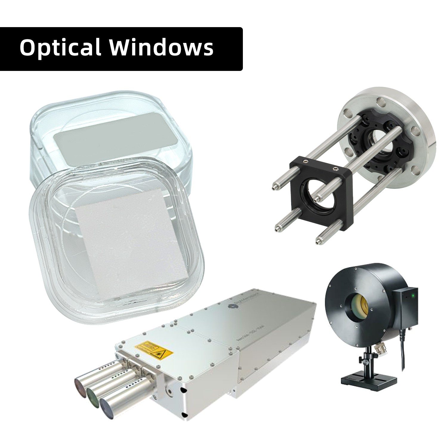

Highlight supplies high-quality, double-side polished single-crystal CVD optical diamond plates with customizable dimensions. Customization options range from 7×7 mm to 25×25 mm for square plates and diameters of Φ8 mm to Φ25 mm for circular plates; standard specifications—such as 10×10×0.4 mm—are also kept in stock to meet most equipment assembly requirements. We also offer one-stop, deep-processing customization services—including doping, high-precision polishing, and surface metallization—tailored to specific project needs and equipment standards. Our products are widely used in high-end precision optics, including optical windows for high-power lasers, infrared detectors, and terahertz systems, ensuring reliable performance for various cutting-edge optical devices.
From the 'razor-sharp edge' on the operating table to the 'cool, steady power' alongside AI chips, and the 'transparent armor' shielding high-energy lasers—CVD diamond is embedding itself deeply into every critical link of modern technology in ways that transcend its role as a mere gemstone.
As a key player in China's CVD diamond sector, Foshan Highlight Intelligent Technology Co., Ltd. has built a product portfolio spanning three major categories—surgical-grade tools, heat-dissipating heat sinks, and optical-grade components—all underpinned by its expertise in the R&D and manufacturing of MPCVD equipment. As production costs fall and application scenarios expand, this 'industrial gem' is set to shine ever more brilliantly.
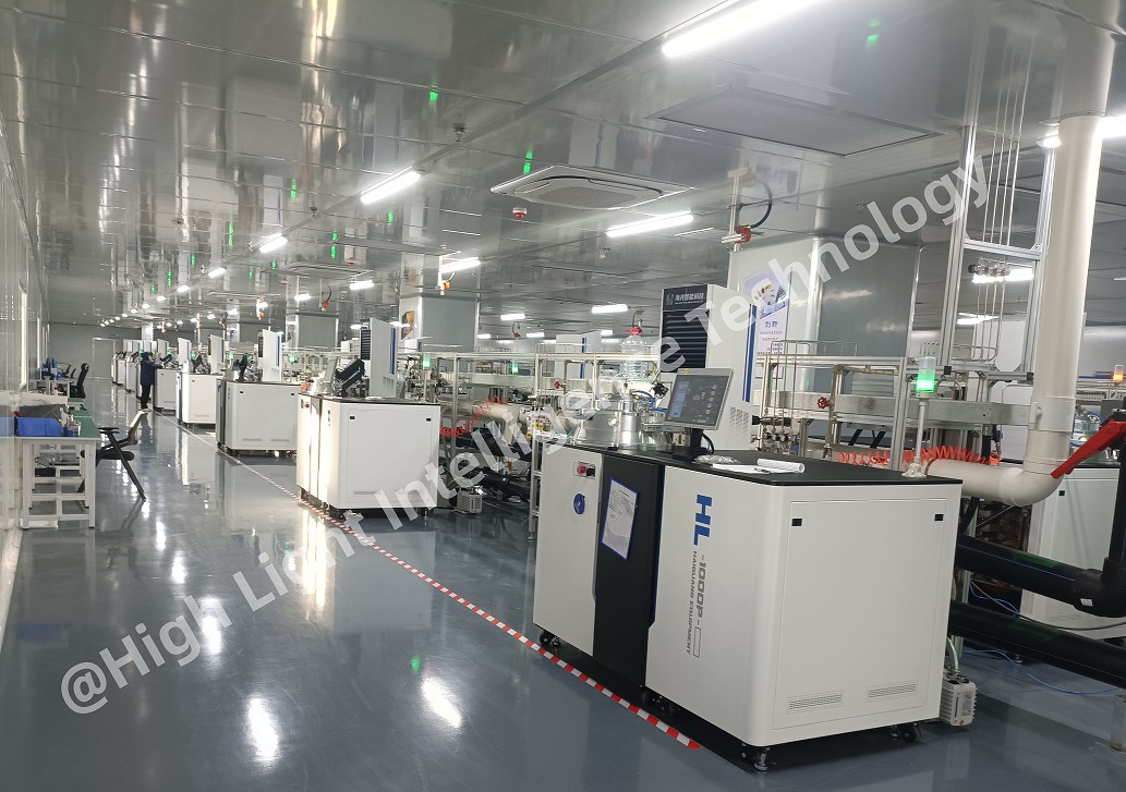
High Light Intelligence Technology, a pioneer in the CVD diamond industry, has advanced MPCVD technology and CVD diamond production workshops. We focus on producing high-purity lab-grown diamonds for the jewelry industry, and at the same time create industrial-grade CVD diamond products, covering single crystals, polycrystalline, films and diamond surface metallization. We also provide 6kw/10kw/15kw MPCVD equipment to help customers in all aspects, from equipment to products, and then to all-round services, to create brilliance together.









-

CVD Single-Crystal Diamonds: An Analysis of the Complete Processing Workflow from Gas-Phase Deposition to Finished Diamond Chips
MPCVD (Microwave Plasma Chemical Vapor Deposition) technology is currently the core process for producing high-quality single-crystal diamond s. Thanks to its advantages of low defect rates, high purity, and controllable large dimensions, it is widely used in fields such as semiconductor heat dissipation, precision optics, and high-end sensors. The final quality of single-crystal diamond s depends on comprehensive process control throughout the entire workflow—from vapor deposition growth to pos
-
Single-Crystal or Polycrystalline Diamond — Which Has Greater Potential?
As diamond continues to enter industries such as semiconductors, thermal management, optics, high-power electronics, and precision machining, the requirements for diamond materials are also evolving.
-
Diamond Polishing and Grinding Processes: Core Challenges and Industry Hurdles
Diamond is often hailed as the “ultimate material” – ranking 10 on the Mohs hardness scale, boasting an ultra‑high thermal conductivity (~2,200 W/(m·K)), excellent chemical stability, and broad optical transparency. These properties make it irreplaceable in cutting‑edge applications such as semiconductor heat dissipation, high‑end optics, and quantum chips. Yet the paradox of “good materials are hard to process” is nowhere more evident than in diamond. From rough grinding for planarization to at
-
Single-Crystal vs Polycrystalline CVD Diamond: Process Difference Lies in Growth Logic, Not Equipment
The process difference between single crystal and polycrystalline CVD diamond lies not in equipment, but in growth logic. Single crystal and polycrystalline CVD diamond are two functional new materials with completely independent growth mechanisms, lattice structures and performance systems. Their process logic, product features and application boundaries diverge fundamentally from the very start of deposition and growth. Comparing or selecting materials without considering their underlying crys




