

- 中文
- English
- Español
A team of academicians from the University of Science and Technology of China achieves high-precision imaging of point defects in diamond
2024-01-19 09:14:37
Click:
“
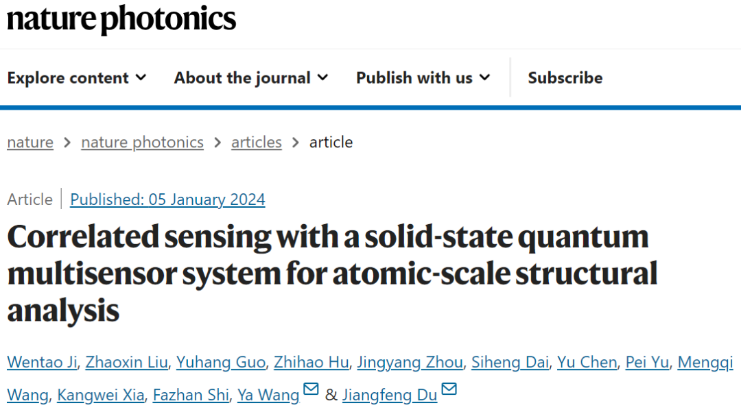
Recently, Du Jiangfeng, Wang Ya and others from the Key Laboratory of Microscopic Magnetic Resonance of the Chinese Academy of Sciences at the University of Science and Technology of China have made important progress in the field of quantum precision measurement, proposing a new quantum sensing paradigm based on signal correlation to achieve high-precision imaging of point defects in diamond. , and observed the charge dynamics of point defects in real time.
”
Recently, Du Jiangfeng, Wang Ya and others from the Key Laboratory of Microscopic Magnetic Resonance of the Chinese Academy of Sciences at the University of Science and Technology of China have made important progress in the field of quantum precision measurement, proposing a new quantum sensing paradigm based on signal correlation to achieve high-precision imaging of point defects in diamond. , and observed the charge dynamics of point defects in real time.
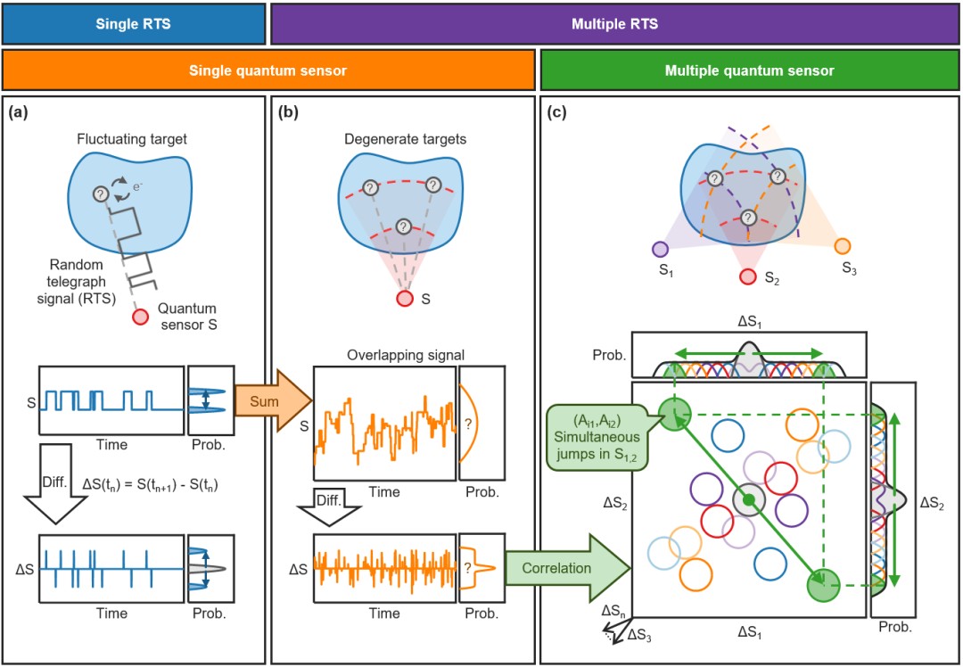
In the past two decades, the development of quantum sensing has made revolutionary progress in the measurement technology of many physical quantities. For example, nanoscale diamond nitrogen-vacancy color center quantum sensors are expected to achieve structural analysis of single molecules. Taking magnetic measurements as an example, the current quantum sensing paradigm to achieve structure resolution requires quantum manipulation of labeled spin detection targets. However, many physical phenomena in nature neither contain spin nor can be directly manipulated, such as random telegraph signals caused by charge dynamics in semiconductors. More importantly, when signals from multiple detection objects overlap and interfere with each other, a single quantum sensor will be unable to effectively extract and analyze the signals.
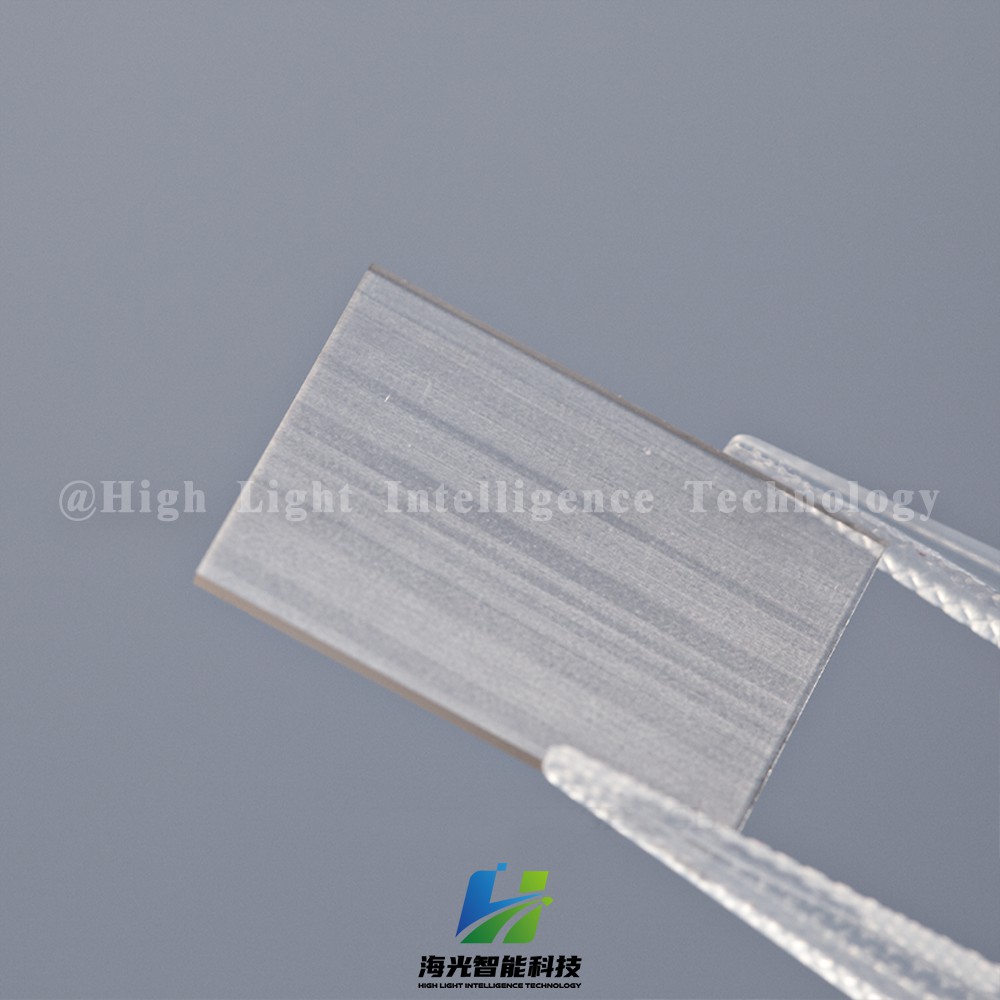
Diamond is a wide-bandgap semiconductor material with excellent properties. The charge dynamics of point defects in the material will bring random electric field noise. In this work, the DC Stark effect of the excited state of diamond nitrogen-vacancy color center is used to realize the sensing of electric field. When the charge state of a point defect changes, three nitrogen-vacancy color centers can simultaneously detect changes in the electric field caused by the change in charge. Using the correlation characteristics of simultaneous changes in the electric field between the three color centers, the electric field corresponding to each point defect can be resolved from the chaotic fluctuation electric field. And since the relative spatial positions of each point defect and the three nitrogen-vacancy color centers are different, the spatial position of the point defect can be accurately located based on the difference in the direction and magnitude of the electric field felt by each nitrogen-vacancy color center. Using this quantum positioning technology, which is similar to satellite positioning, the research team successfully located 16 point defects within the micron range, with a maximum positioning accuracy of 1.7 nanometers. Based on this ability of correlation resolution and precise positioning, the research team also achieved in-situ real-time detection of the charge dynamics of each point defect, providing a new method for studying the properties of point defects within bulk materials.
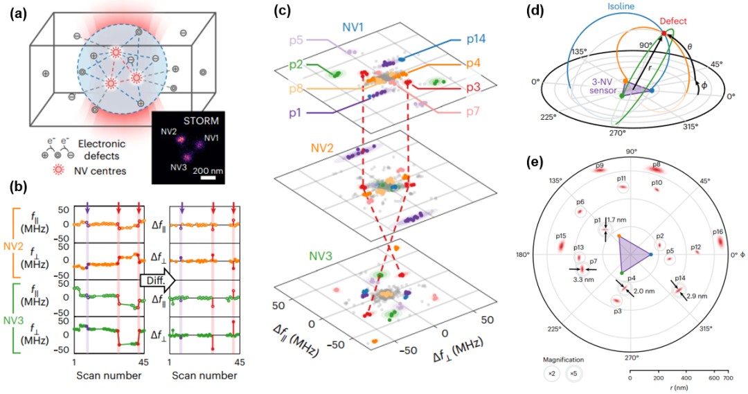
Figure: (a) Schematic diagram of the experimental system. The small picture shows the super-resolution imaging of the three-color center system used in this work; (b) The fluctuation of the peak position of the resonance fluorescence excitation spectrum corresponds to the electric field at each color center. Fluctuations; (c) Different defects can be distinguished by using the correlation between the electric field fluctuation signals of the three color centers; (d) Schematic diagram of the quantum positioning system; (e) 16 positioned around the three color centers Point defects.
Ji Wentao, special associate researcher of the Key Laboratory of Microscopic Magnetic Resonance, and doctoral candidates Liu Zhaoxin and Guo Yuhang are the co-first authors of this work, and Academician Du Jiangfeng and Professor Wang Ya are the co-corresponding authors. This research was funded by the National Natural Science Foundation of China, the Chinese Academy of Sciences, the Ministry of Science and Technology, and Anhui Province
As a semiconductor diamond production supplier, High Light Intelligence Technology is developing rapidly in the semiconductor industry. We also provide diamond materials to major commercial customers and academic researchers, contributing to the development of semiconductor technology and materials.With MPCVD technology as the core, we have long been committed to the R&D and manufacturing of high-quality diamond materials and related equipment. We have advanced MPCVD equipment, laser processing equipment and precision polishing equipment.









-

CVD Single-Crystal Diamonds: An Analysis of the Complete Processing Workflow from Gas-Phase Deposition to Finished Diamond Chips
MPCVD (Microwave Plasma Chemical Vapor Deposition) technology is currently the core process for producing high-quality single-crystal diamond s. Thanks to its advantages of low defect rates, high purity, and controllable large dimensions, it is widely used in fields such as semiconductor heat dissipation, precision optics, and high-end sensors. The final quality of single-crystal diamond s depends on comprehensive process control throughout the entire workflow—from vapor deposition growth to pos
-
Single-Crystal or Polycrystalline Diamond — Which Has Greater Potential?
As diamond continues to enter industries such as semiconductors, thermal management, optics, high-power electronics, and precision machining, the requirements for diamond materials are also evolving.
-
Diamond Polishing and Grinding Processes: Core Challenges and Industry Hurdles
Diamond is often hailed as the “ultimate material” – ranking 10 on the Mohs hardness scale, boasting an ultra‑high thermal conductivity (~2,200 W/(m·K)), excellent chemical stability, and broad optical transparency. These properties make it irreplaceable in cutting‑edge applications such as semiconductor heat dissipation, high‑end optics, and quantum chips. Yet the paradox of “good materials are hard to process” is nowhere more evident than in diamond. From rough grinding for planarization to at
-
Single-Crystal vs Polycrystalline CVD Diamond: Process Difference Lies in Growth Logic, Not Equipment
The process difference between single crystal and polycrystalline CVD diamond lies not in equipment, but in growth logic. Single crystal and polycrystalline CVD diamond are two functional new materials with completely independent growth mechanisms, lattice structures and performance systems. Their process logic, product features and application boundaries diverge fundamentally from the very start of deposition and growth. Comparing or selecting materials without considering their underlying crys




