

- 中文
- English
- Español
The world's first! Diamond transistor!
2024-03-27 09:18:57
Click:
“
Diamond has the highest figure of merit of any known semiconductor used in next-generation electronic devices, far exceeding the performance of conventional semiconductor silicon. To realize diamond integrated circuits, the development of diamond complementary metal-oxide semiconductor (CMOS) devices requires n-channel and p-channel conductivity, just like devices built for the semiconductor silicon. However, diamond CMOS was never realized due to challenges with n-channel MOS field-effect trans
”
Among all known semiconductors, diamond significantly surpasses the traditional semiconductor silicon with its excellent quality factor, providing a promising material choice for the next generation of electronic devices. However, for diamond to be used in integrated circuit fabrication, diamond complementary metal oxide semiconductor (CMOS) devices must be developed with n-channel and p-channel conductivity, the same device construction principles we have established for the semiconductor silicon . Unfortunately, due to technical difficulties in n-channel metal oxide semiconductor field effect transistors (MOSFETs), the research and development of diamond CMOS has not been able to achieve a breakthrough.
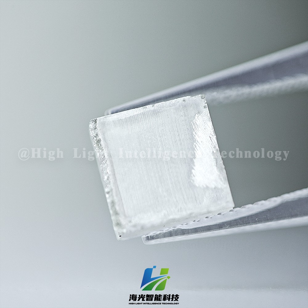
Recently, researchers at Japan's National Institute of Materials Science (NIMS) have made breakthrough progress. Based on the step flow nucleation mode, they successfully fabricated an electronically graded phosphorus-doped n-type diamond epitaxial layer with an atomically flat surface and demonstrated an n-channel diamond MOSFET. This n-type diamond MOSFET exhibits a field-effect mobility of approximately 150 cm²/V·s at 573 K, which ranks first among all n-channel MOSFETs based on wide-bandgap semiconductors. This major achievement not only helps promote the research and development of diamond CMOS integrated circuits, but also opens up new paths in the development of energy-saving and highly reliable electronic devices, integrated spin electronics and extreme sensors, especially in harsh environments. It shows great potential in applications requiring high-power electronic devices.

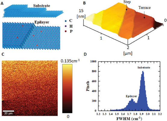
Figure 1. High-quality lightly phosphorus-doped n-type diamond epitaxial layer.
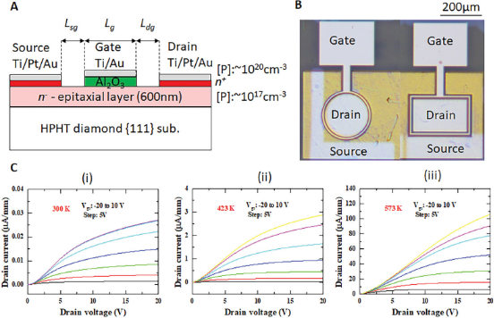
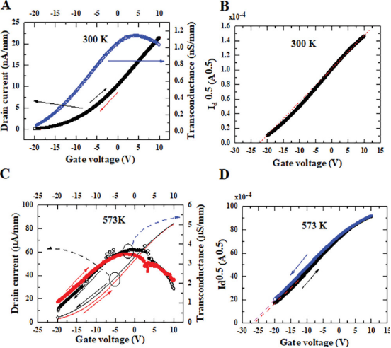
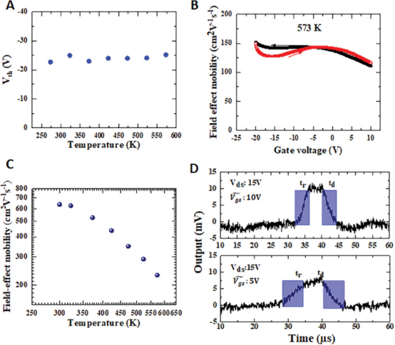
1. The NIMS research team developed the world's first n-channel diamond MOSFET (Metal Oxide Semiconductor Field Effect Transistor). The developed n-channel diamond MOSFET is a key step in the development of CMOS (complementary metal oxide semiconductor: one of the most popular technologies in computer chips) integrated circuits and diamond power electronics for harsh environment applications.
2. Semiconductor diamond has excellent physical properties such as ultra-wide bandgap energy of 5.5eV, high carrier mobility, and high thermal conductivity. It has high performance and high reliability application prospects in extreme environmental conditions such as high temperature and high radiation. horizontal (e.g., near a nuclear reactor core). By using diamond electronics, not only are the thermal management needs of traditional semiconductors alleviated, but these devices are also more energy efficient and can withstand higher breakdown voltages and harsh environments. On the other hand, with the development of diamond growth technology, power electronics, spin electronics, and microelectromechanical systems (MEMS) sensors that can operate under high temperature and strong radiation conditions, there is a constant demand for peripheral circuits based on diamond CMOS devices. Increase. Integration. For the fabrication of CMOS integrated circuits, as with conventional silicon electronics, p- and n-channel MOSFETs are required. However, n-channel diamond MOSFETs have not yet been developed.

3. The NIMS research team developed a technology to grow high-quality single-crystal n-type diamond semiconductors with smooth and flat platforms at the atomic level by doping diamond with low concentrations of phosphorus. Using this technology, the team successfully manufactured n-channel diamond MOSFETs for the first time in the world. The MOSFET is mainly composed of an n-channel diamond semiconductor layer and another diamond layer doped with a high concentration of phosphorus. The use of the latter diamond layer significantly reduces source and drain contact resistance. The team confirmed that the diamond MOSFETs produced actually functioned as N-channel transistors. In addition, the team also verified the excellent high-temperature performance of the MOSFET, with its field-effect mobility, an important performance indicator of transistors, of approximately 150 cm2/V・sec at 300°C.
4. These results are expected to facilitate the development of CMOS integrated circuits for manufacturing energy-saving power electronics, spintronics, and (MEMS) sensors in harsh environments.










-

CVD Single-Crystal Diamonds: An Analysis of the Complete Processing Workflow from Gas-Phase Deposition to Finished Diamond Chips
MPCVD (Microwave Plasma Chemical Vapor Deposition) technology is currently the core process for producing high-quality single-crystal diamond s. Thanks to its advantages of low defect rates, high purity, and controllable large dimensions, it is widely used in fields such as semiconductor heat dissipation, precision optics, and high-end sensors. The final quality of single-crystal diamond s depends on comprehensive process control throughout the entire workflow—from vapor deposition growth to pos
-
Single-Crystal or Polycrystalline Diamond — Which Has Greater Potential?
As diamond continues to enter industries such as semiconductors, thermal management, optics, high-power electronics, and precision machining, the requirements for diamond materials are also evolving.
-
Diamond Polishing and Grinding Processes: Core Challenges and Industry Hurdles
Diamond is often hailed as the “ultimate material” – ranking 10 on the Mohs hardness scale, boasting an ultra‑high thermal conductivity (~2,200 W/(m·K)), excellent chemical stability, and broad optical transparency. These properties make it irreplaceable in cutting‑edge applications such as semiconductor heat dissipation, high‑end optics, and quantum chips. Yet the paradox of “good materials are hard to process” is nowhere more evident than in diamond. From rough grinding for planarization to at
-
Single-Crystal vs Polycrystalline CVD Diamond: Process Difference Lies in Growth Logic, Not Equipment
The process difference between single crystal and polycrystalline CVD diamond lies not in equipment, but in growth logic. Single crystal and polycrystalline CVD diamond are two functional new materials with completely independent growth mechanisms, lattice structures and performance systems. Their process logic, product features and application boundaries diverge fundamentally from the very start of deposition and growth. Comparing or selecting materials without considering their underlying crys




