

- 中文
- English
- Español
Xiamen University and Huawei Cooperation: A New Breakthrough in Diamond Cooling!
2024-03-29 09:49:13
Click:
“
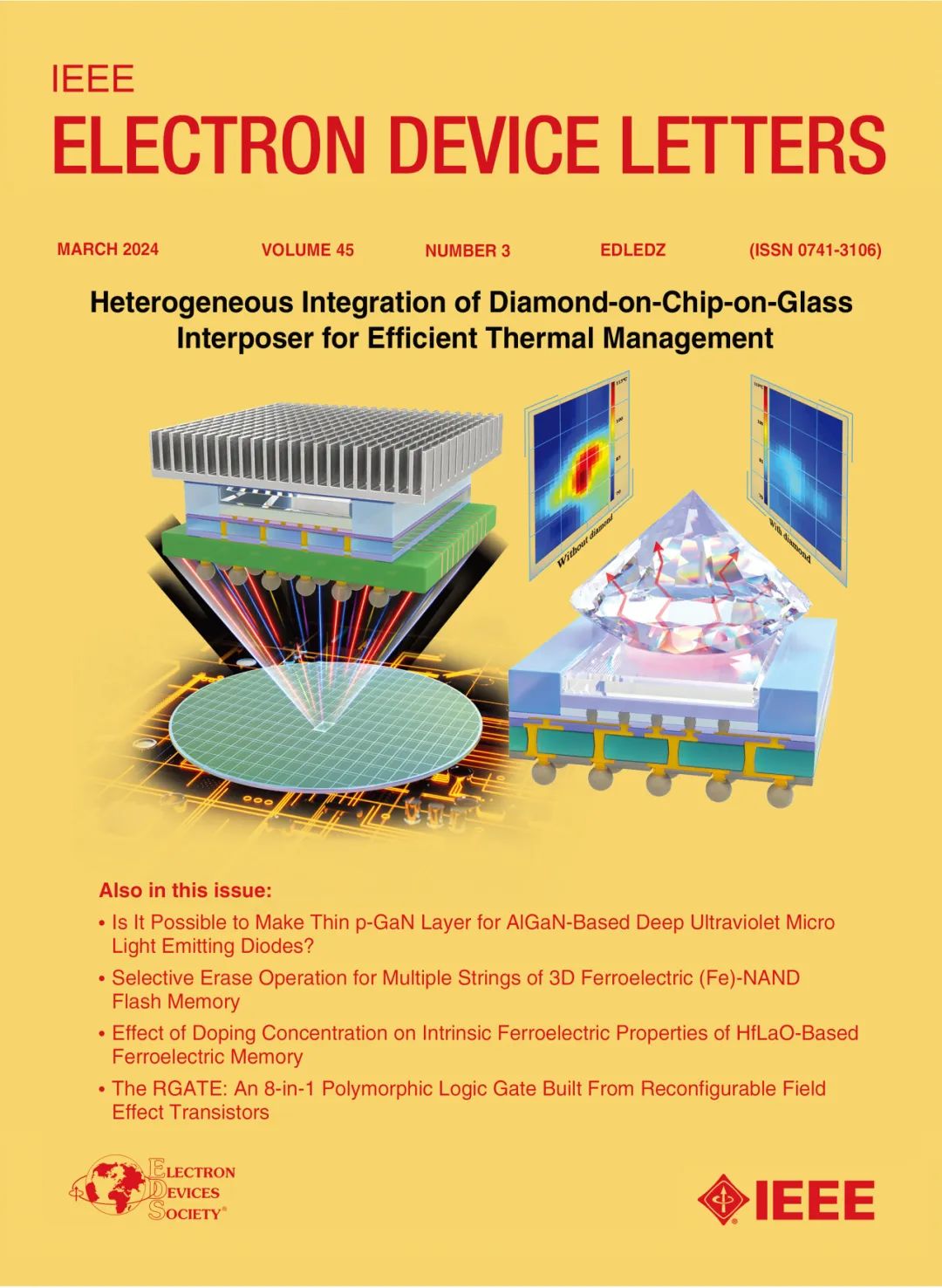
Recently, the School of Electronic Science and Technology at Xiamen University, along with Huawei and Xiamen Yuntian teams, made a breakthrough in the field of integrated chip diamond heat dissipation technology for packaged glass adapters. The related achievements were published in the authoritative journal IEEE Electron Device Letters in the field of microelectronic device packaging and manufacturing, with the title "Heterogeneous Integration of Diamond on Chip on Glass Interposer for Efficien
”
Recently, a team led by Professor Yu Daquan and Professor Zhong Yi from the School of Electronic Science and Technology at Xiamen University, in collaboration with Huawei and the Xiamen Yuntian team, made breakthrough progress in the field of advanced packaging glass adapter integrated chip diamond heat dissipation technology. The related achievements were published in the international authoritative journal IEEE Electron Device Letters in the field of microelectronic device packaging and manufacturing under the title of "Heterogeneous Integration of Diamond on Chip on Glass Interposer for Efficient Thermal Management", and were selected as the front cover and editors' Picks for the current period.
With the rapid development of AI technology and its enormous demand for computing power, 2.5D and 3D packaging technologies are receiving increasing attention. Compared to silicon adapter plates, 2.5D packaging using glass adapter plates has the following advantages: 1) excellent high-frequency electrical characteristics; 2) Large and ultra-thin glass substrates are easy to obtain; 3) The process flow is simple, and there is no need to make a through hole side wall insulation layer; 4) The low-cost advantage brought by large-sized substrates and simplified process flow. On the other hand, whether using silicon or glass adapters for 2.5D packaging, as well as 3D integration of multiple active chip stacks, the higher integration density and power density pose serious challenges to chip thermal management. The current cooling technology mainly relies on hot through-holes, uniform heat plates, forced air or liquid cooling, which result in larger external dimensions and significant energy consumption at the packaging or board level.
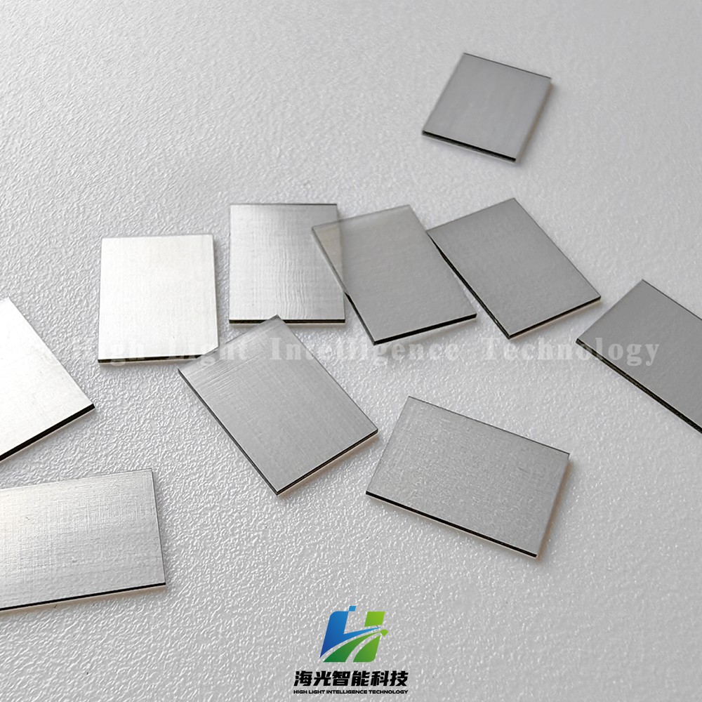
Diamond has a very high isotropic thermal conductivity (1000-2200 W/(mK)) and has broad prospects as a heat sink. At present, the artificial synthesis of diamond is limited to 5-inch wafers, resulting in its wafer level integration with semiconductor substrates being limited to smaller III-V group semiconductors and compound semiconductors (GaN, SiC); In addition, the growth temperature of artificial diamond exceeds 400 ℃, which can easily cause damage to the chip. Chip level integration can avoid the problems of small wafer size and high growth temperature. However, traditional chip bonding techniques, such as soldering and silver sintering, often introduce thicker solder layers, resulting in larger interfacial thermal resistance. There is an urgent need for a chip level diamond integration process with low temperature, low stress, and low interface thermal resistance.
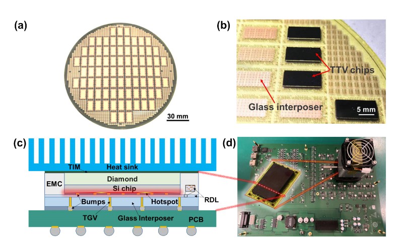
Figure 1. (a) 6-inch glass adapter plate with glass through holes (TGV) and redistribution layers (RDLs) for diamond/chip packaging, (b) chip bonded to glass adapter plate wafer, (c) schematic diagram of integrated diamond chip glass adapter plate (DoCoG), and (d) photos of DoCoG packaging thermal testing configuration.
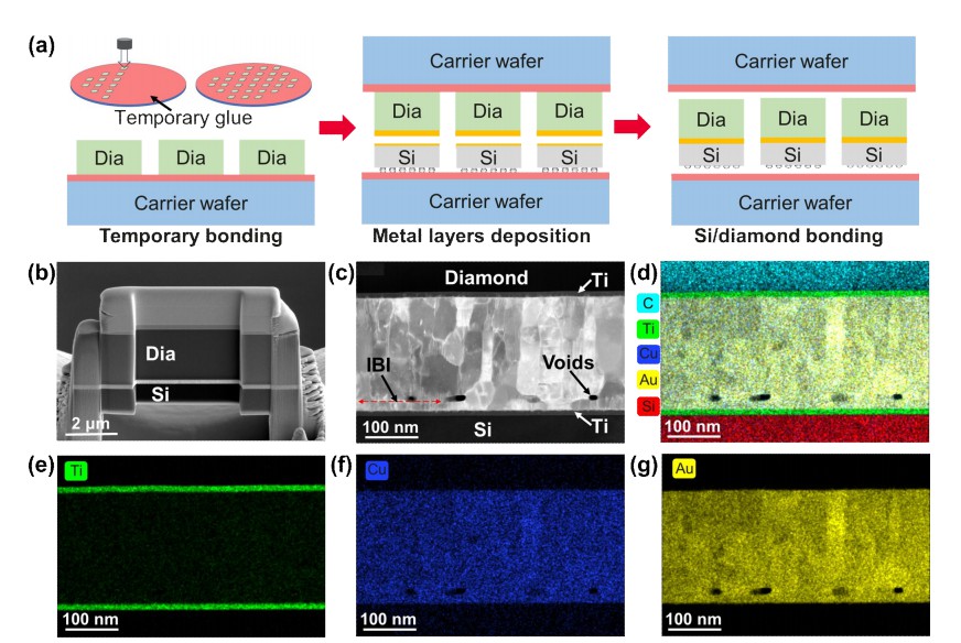
Figure 2. (a) Schematic diagram of bonding process between diamond and thermal testing chip with micro protrusions, (b) SEM and (c) TEM analysis of diamond/silicon bonding interface, and (d)~(g) EDS distribution of C, Si, Ti, Cu, and Au elements.
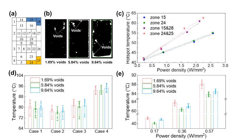
Figure 3. (a) There are 28 independently controllable heating areas on the thermal testing chip, (b) voids at the bonding interface of the diamond/thermal testing chip, (c) maximum hot spot temperature at different power densities, (d) and (e) measurement temperatures for local high heat flux heating and global uniform heat flux heating at different bonding porosity, respectively.
This study innovatively integrates diamond low-temperature bonding and glass adapter plate technology, successfully integrating polycrystalline diamond substrates on the back of glass adapter plate chips for the first time. It not only conforms to the trend of miniaturization and lightweighting of electronic devices, but also becomes a breakthrough path for efficient chip heat dissipation, promoting the industrialization process of diamond heat dissipation substrates in the field of advanced packaging. At the same time, the team conducted in-depth research on glass substrate passive device technology and diamond substrate heat dissipation technology, providing strong support for high-performance, high integration, and low-cost three-dimensional integration of microsystems.
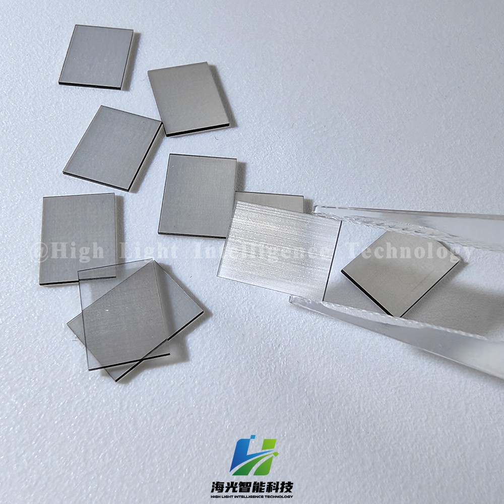
With MPCVD technology as its core, High Light Intelligence Technology has long been committed to the R&D and manufacturing of high-quality diamond materials and related equipment. It has advanced MPCVD equipment, laser processing equipment and precision polishing equipment. High Light Intelligence Technology's MPCVD technology equipment can produce high-quality diamond, thereby helping to improve the performance of integrated circuits. Our products and services are designed to provide customers with the best solutions to meet their needs for high quality diamond and integrated circuit performance.









-

CVD Single-Crystal Diamonds: An Analysis of the Complete Processing Workflow from Gas-Phase Deposition to Finished Diamond Chips
MPCVD (Microwave Plasma Chemical Vapor Deposition) technology is currently the core process for producing high-quality single-crystal diamond s. Thanks to its advantages of low defect rates, high purity, and controllable large dimensions, it is widely used in fields such as semiconductor heat dissipation, precision optics, and high-end sensors. The final quality of single-crystal diamond s depends on comprehensive process control throughout the entire workflow—from vapor deposition growth to pos
-
Single-Crystal or Polycrystalline Diamond — Which Has Greater Potential?
As diamond continues to enter industries such as semiconductors, thermal management, optics, high-power electronics, and precision machining, the requirements for diamond materials are also evolving.
-
Diamond Polishing and Grinding Processes: Core Challenges and Industry Hurdles
Diamond is often hailed as the “ultimate material” – ranking 10 on the Mohs hardness scale, boasting an ultra‑high thermal conductivity (~2,200 W/(m·K)), excellent chemical stability, and broad optical transparency. These properties make it irreplaceable in cutting‑edge applications such as semiconductor heat dissipation, high‑end optics, and quantum chips. Yet the paradox of “good materials are hard to process” is nowhere more evident than in diamond. From rough grinding for planarization to at
-
Single-Crystal vs Polycrystalline CVD Diamond: Process Difference Lies in Growth Logic, Not Equipment
The process difference between single crystal and polycrystalline CVD diamond lies not in equipment, but in growth logic. Single crystal and polycrystalline CVD diamond are two functional new materials with completely independent growth mechanisms, lattice structures and performance systems. Their process logic, product features and application boundaries diverge fundamentally from the very start of deposition and growth. Comparing or selecting materials without considering their underlying crys




