

- 中文
- English
- Español
Where is the development direction of diamond homoepitaxial growth technology? Kanazawa University in Japan provides the answer with its research on excellent growth rate
2024-09-13 09:04:59
Click:
“
Strong covalent bonds endow diamond with excellent properties, such as high thermal conductivity, high mobility and wide bandgap, making it a candidate material for power devices, optoelectronics, quantum technology and sensors. However, practical applications still face challenges, such as MPCVD process control to achieve large size, smooth surface and conductivity requirements, as well as the improvement of traditional processing technology. This article outlines three MPCVD growth technology
”
01
The paper introduces the technology of diamond sheet growth rate enhancement. By optimizing the reactor, electric field, gas and substrate positioning of MPCVD, a high growth rate of 250 μm/h and excellent crystal quality are achieved without nitrogen. After adding nitrogen and optimizing the conditions, the rate is increased to 432 μm/h. This technology produces 0.1mm thick independent diamond plates with crystallinity comparable to HPHT substrates and better than commercial CVD substrates. X-ray diffraction verifies its high quality. However, the application of large-area substrates is still a technical difficulty.
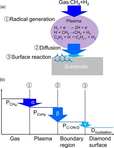
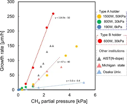
Key points of diamond CVD growth: Free radicals are generated by microwave excitation of hydrogen-methane mixture; hydrogen atoms promote the preservation of active substances. Active substances diffuse from plasma to substrate, collide on the way to generate new substances, and interact with the diamond surface through the sheath. During the surface reaction, active substances migrate to the reaction site to form chemical bonds or desorb, hydrogen atoms etch SP2 bonds, and hydrocarbons promote diamond growth. The study used CVD equipment and support structure to explore the growth rate of (100) diamond film as a function of methane partial pressure, and found that increasing microwave power and total pressure can increase the growth rate, up to 150μm/h. High power density may improve methane conversion efficiency, but the growth rate slope is equivalent to that under nitrogen-free conditions, which may be attributed to the low diffusion efficiency of carbon free radicals.
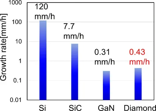
The research report pointed out that the project has achieved the fastest growth rate in the world. Compared with power semiconductor materials such as Si, SiC and GaN, the growth rate of diamond is lower than that of commercial Si and SiC, but it is comparable to GaN. The biggest challenge is to expand the area of diamond seeds. Heteroepitaxial growth is difficult to reach a large size, and homoepitaxial growth can be three-dimensional or mosaic growth. The team's technology has been successfully tested on a small substrate and is suitable for the latter. MPCVD requires three-dimensional expansion of the plasma ball to increase the area, but reduces the power density and limits the growth rate over a large area. Although 915 MHz microwaves increase the area, they reduce power utilization and material supply efficiency. The solution lies in two-dimensional expansion of plasma to increase power density, and explore hot filament CVD and plasma-free gas CVD to reduce the energy cost of diamond production.
02
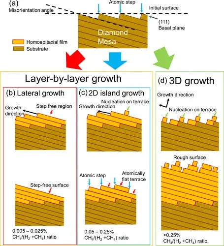
The researchers manipulated the diamond surface at the atomic level by adjusting the growth mode. On the homoepitaxial (111) surface, lateral, two-dimensional island and three-dimensional growth modes were used. By finely controlling the methane concentration and substrate misalignment, the growth mode can be switched on the high-pressure and high-temperature (111) table. The lateral growth was extended from microns to millimeters. After optimization, the researchers achieved an atomically flat diamond surface on the entire substrate.
03









-

Foshan Highlight Intelligent Technology invites you to the 140th Canton Fair—join us at Booth 21.2A23-24 in the Friendship Hall to share in the brilliance.
Foshan Highlight Intelligent Technology invites you to the 140th Canton Fair—join us at Booth 21.2A23-24 in the Friendship Hall to share in the brilliance.
-
CVD Single-Crystal Diamonds: An Analysis of the Complete Processing Workflow from Gas-Phase Deposition to Finished Diamond Chips
MPCVD (Microwave Plasma Chemical Vapor Deposition) technology is currently the core process for producing high-quality single-crystal diamond s. Thanks to its advantages of low defect rates, high purity, and controllable large dimensions, it is widely used in fields such as semiconductor heat dissipation, precision optics, and high-end sensors. The final quality of single-crystal diamond s depends on comprehensive process control throughout the entire workflow—from vapor deposition growth to pos
-
Single-Crystal or Polycrystalline Diamond — Which Has Greater Potential?
As diamond continues to enter industries such as semiconductors, thermal management, optics, high-power electronics, and precision machining, the requirements for diamond materials are also evolving.
-
Diamond Polishing and Grinding Processes: Core Challenges and Industry Hurdles
Diamond is often hailed as the “ultimate material” – ranking 10 on the Mohs hardness scale, boasting an ultra‑high thermal conductivity (~2,200 W/(m·K)), excellent chemical stability, and broad optical transparency. These properties make it irreplaceable in cutting‑edge applications such as semiconductor heat dissipation, high‑end optics, and quantum chips. Yet the paradox of “good materials are hard to process” is nowhere more evident than in diamond. From rough grinding for planarization to at




