

- 中文
- English
- Español
Analysis of the diverse application areas of diamond
2024-10-23 09:39:23
Click:
“
Diamond has excellent electrical properties, wide bandgap, high breakdown, and high mobility, making it suitable as the ultimate semiconductor; acoustically, it has the fastest sound wave speed and a high Young's modulus; it is optically transparent to the far infrared and ultraviolet; its thermal conductivity exceeds that of copper, and it has broad application potential.
”
Diamond has excellent electrical properties, a wide bandgap, high breakdown field strength and high mobility, and is expected to become the ultimate semiconductor. Acoustically, it has the fastest surface acoustic wave speed and an extremely high Young's modulus. Its optical transparency range is as wide as far infrared to ultraviolet. Its thermal conductivity exceeds that of copper, and it has cross-field application potential.

Synthesis of functional diamond:
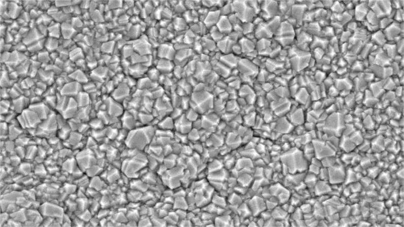
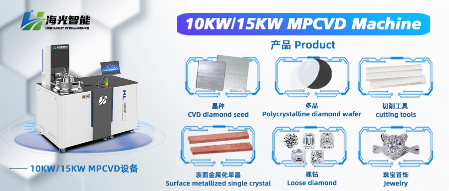
Compared with traditional HPHT diamond synthesis, functional diamond mainly adopts atmospheric pressure CVD method. CVD diamond is divided into thin film (<50μm, including conventional and nanofilm) and self-supporting thick film (single crystal, polycrystalline). According to the synthesis technology, it is divided into microwave assisted (MPCVD), hot wire and DC type, among which MPCVD is the mainstream high-quality synthesis method.
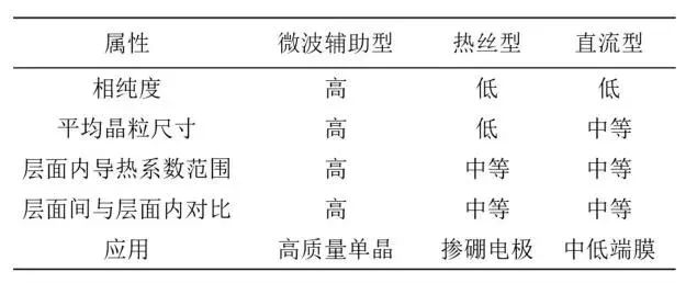
Application of Functional Diamond
Jewelry Grade Applications
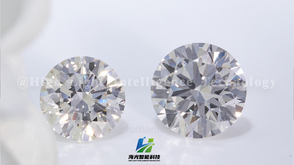
High temperature and high pressure (HTHP) is the main method for producing lab-grown diamonds. The chemical vapor deposition (CVD) method for producing lab-grown diamonds has made rapid progress in the past three years, with a significant reduction in costs and significant progress in process stability. It has been mass-produced and put on the market in industrial batches.
Semiconductor Applications
As the "ultimate semiconductor", diamond is suitable for manufacturing high-performance electronic devices, with properties far exceeding those of GaN and SiC. It can emit high-intensity free excitons, which helps deep ultraviolet technology. Single crystal growth and doping technology are key. In the future, it is expected to break through technical bottlenecks and achieve better performance. Diamond semiconductor devices may become industry standards, with a wide range of impacts, including computers, automobiles, aerospace, etc.
Thermal Applications
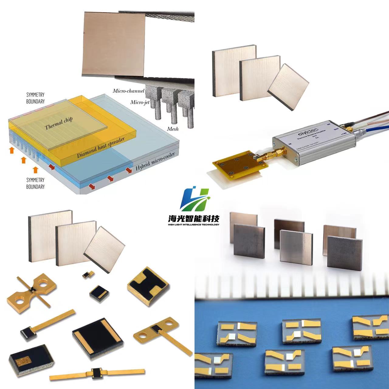
Diamond has an extremely high thermal conductivity (2200W/(m·K)), far exceeding SiC, Si, GaAs and metals, and has a low thermal expansion coefficient and high elastic modulus, making it a high-quality electronic packaging material. It has been used in diamond-enhanced metal packaging and heat sink-diamond substrate GaN devices, etc., with commercial thermal conductivity of 350~600W/(m·K). The price of artificial diamond has dropped, which is conducive to large-scale production. Its high thermal conductivity and electrical insulation make it an optimal heat sink for high-power devices, such as laser diodes. CVD diamond and GaN integration has been achieved to improve RF power density.
Optical Applications
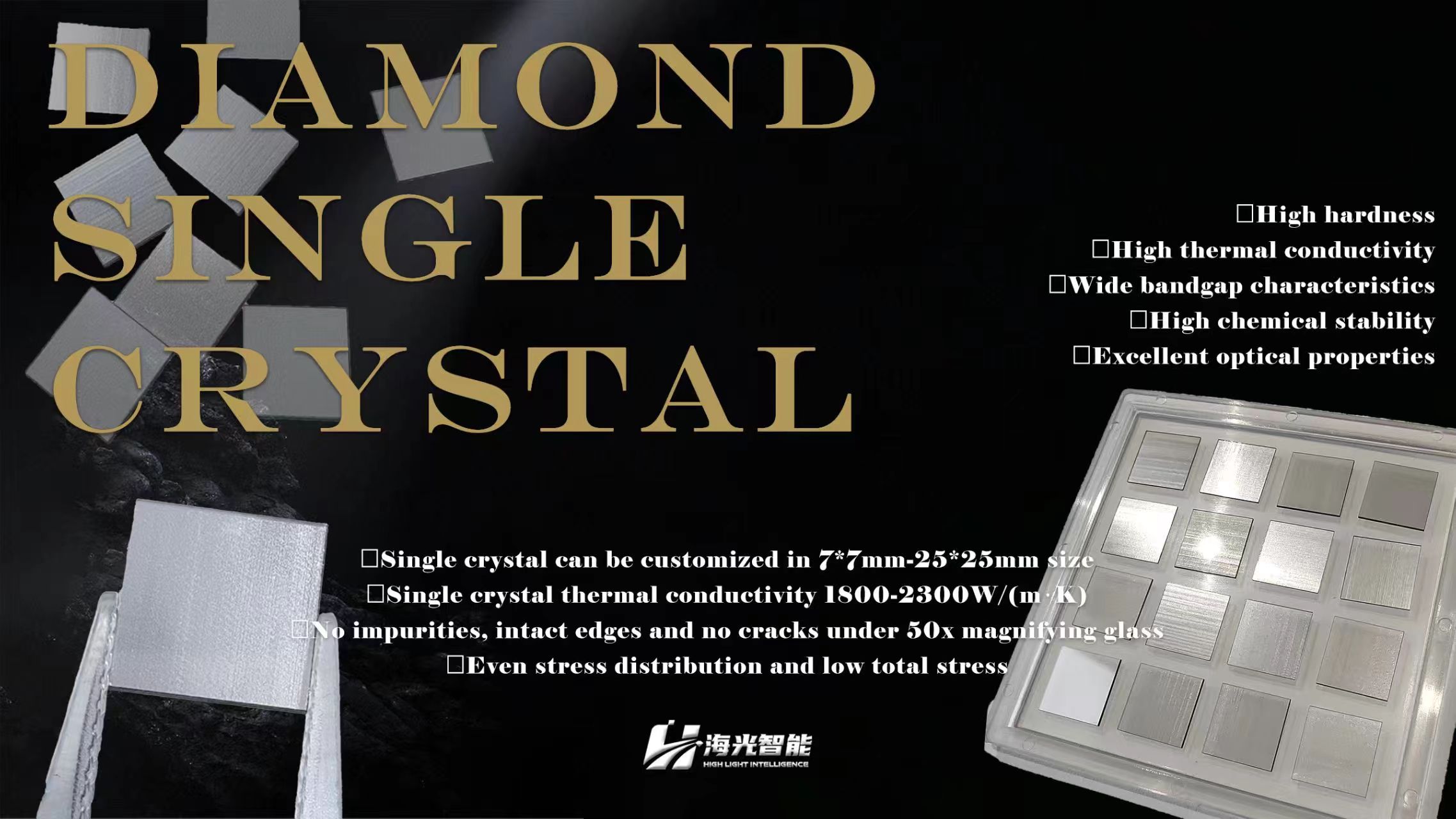
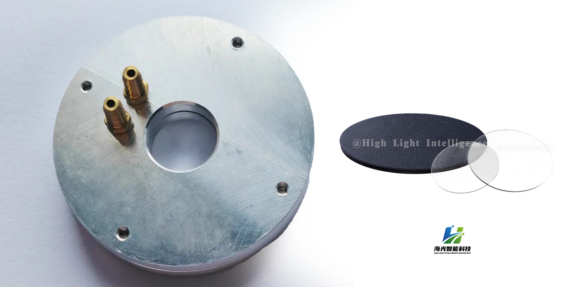
An ideal power transmission window must have: low total absorption, low thermal expansion coefficient, high thermal conductivity, high strength and Young's modulus, and small temperature change of refractive index. Diamond meets almost all of these requirements. Polycrystalline diamond has been industrialized in the fields of optical windows and is also used for decoration, such as high-end watches, luxury coatings and fashion products. Its strength and hardness far exceed Corning glass, and it is also used in mobile phone screens and camera lenses.
Acoustic Devices
Diamond has low density and high strength, and is a high-performance high-frequency acoustic material that can vibrate perfectly at 70kHz to achieve excellent sound reproduction. It has the highest surface acoustic wave velocity and is the preferred material for surface acoustic wave filters, improving filtering frequency and power handling capacity.

Boron-doped diamond (BDD) electrode
Research shows that BDD is an environmentally friendly new electrode material. The electrochemical method has a remarkable effect on treating refractory organic matter and can almost completely mineralize it, which has attracted much attention. The BDD electrode generates strong oxidizing hydroxyl radicals and efficiently degrades wastewater organic matter. It has a wide electrochemical window, high oxygen evolution potential, and strong chemical stability. It is suitable for harsh environments and is expected to become a top organic wastewater treatment technology.
Applications of Quantum Technology
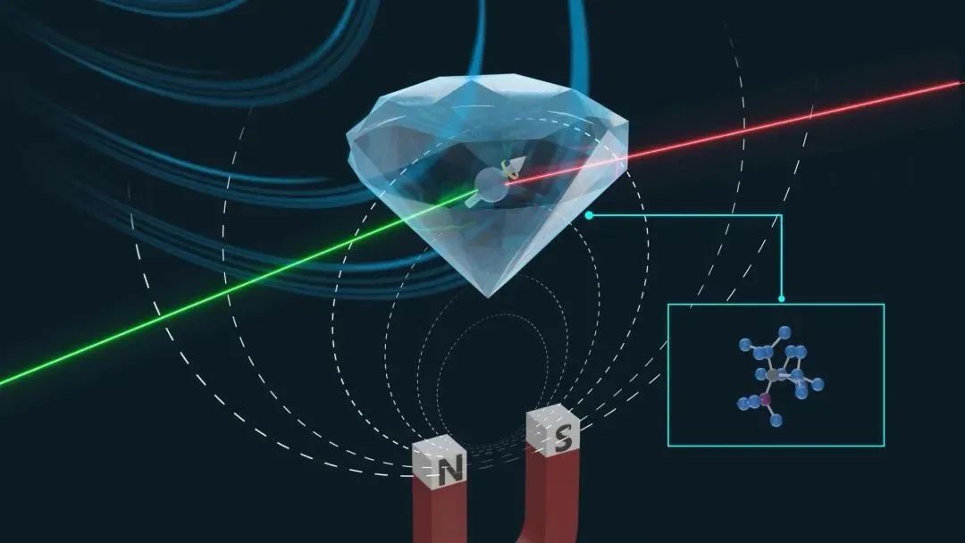
Diamond quantum technology helps solve biomedical and information economy problems. Diamond nitrogen vacancy defects are transformed into quantum resources and controlled by light at room temperature. Artificial diamonds are used as traps, impurities can be controlled, and photons can read information. Diamonds are developed into medical interfaces due to their characteristics, coatings are used for equipment, large-size blades are made, and nanoscale drug delivery labels can be used.
Applications of Quantum Technology
Nanodiamond has a large surface area, rich functional groups, easy adsorption reaction, and good dispersion after treatment. Experiments have proven that adding one thousandth of a spherical nanodiamond to lubricating oil can significantly improve the anti-wear and shock-absorbing effect and is widely suitable for mechanical structures.









-

Foshan Highlight Intelligent Technology invites you to the 140th Canton Fair—join us at Booth 21.2A23-24 in the Friendship Hall to share in the brilliance.
Foshan Highlight Intelligent Technology invites you to the 140th Canton Fair—join us at Booth 21.2A23-24 in the Friendship Hall to share in the brilliance.
-
CVD Single-Crystal Diamonds: An Analysis of the Complete Processing Workflow from Gas-Phase Deposition to Finished Diamond Chips
MPCVD (Microwave Plasma Chemical Vapor Deposition) technology is currently the core process for producing high-quality single-crystal diamond s. Thanks to its advantages of low defect rates, high purity, and controllable large dimensions, it is widely used in fields such as semiconductor heat dissipation, precision optics, and high-end sensors. The final quality of single-crystal diamond s depends on comprehensive process control throughout the entire workflow—from vapor deposition growth to pos
-
Single-Crystal or Polycrystalline Diamond — Which Has Greater Potential?
As diamond continues to enter industries such as semiconductors, thermal management, optics, high-power electronics, and precision machining, the requirements for diamond materials are also evolving.
-
Diamond Polishing and Grinding Processes: Core Challenges and Industry Hurdles
Diamond is often hailed as the “ultimate material” – ranking 10 on the Mohs hardness scale, boasting an ultra‑high thermal conductivity (~2,200 W/(m·K)), excellent chemical stability, and broad optical transparency. These properties make it irreplaceable in cutting‑edge applications such as semiconductor heat dissipation, high‑end optics, and quantum chips. Yet the paradox of “good materials are hard to process” is nowhere more evident than in diamond. From rough grinding for planarization to at




