

- 中文
- English
- Español
Diamond semiconductors, worth looking forward to!
2025-01-08 09:32:22
Click:
“
Diamond has long been regarded as a symbol of luxury and hardness, and its unique physical and chemical properties have earned it the reputation of "the ultimate semiconductor material". As a semiconductor material, diamond has an amazing combination of properties.
”
Diamond has long been regarded as a symbol of luxury and hardness, and its unique physical and chemical properties have earned it the reputation of "the ultimate semiconductor material". As a semiconductor material, diamond has an amazing combination of properties.
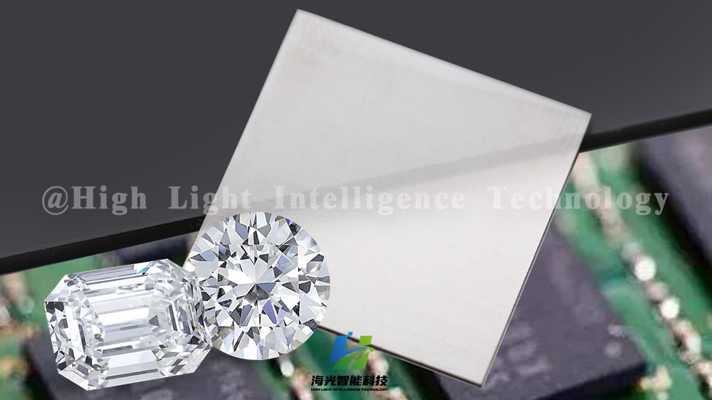
Characteristic
Wide Band Gap
High Speed
High Thermal Conductivity
Diamond has a high thermal conductivity, up to 2300 W/(m·K), far exceeding copper and silicon, making it an ideal heat dissipation material.

Protect Against Radiation

Strong Light Transmittance
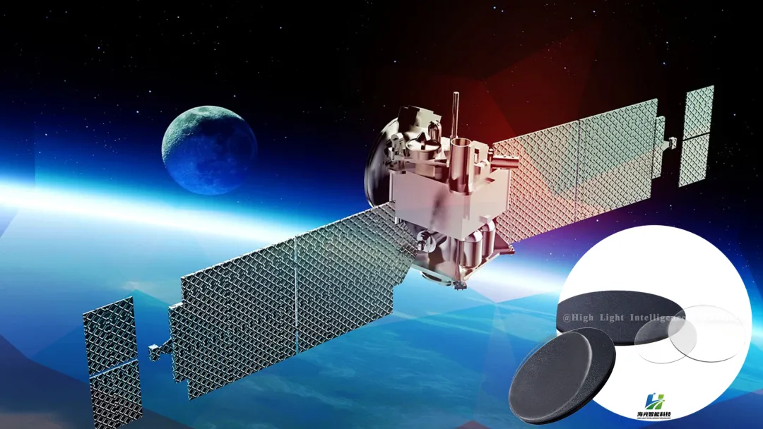
Application prospects
1
High power electronic devices

2
Electric vehicles and green energy

3
Power electronics equipment

4
Optical field
Challenges & Prospects
Although diamond semiconductors have advantages, they still face challenges: such as high prices, complex synthesis, difficult processing and n-type doping technology problems, which limit their popularity. However, scientific and technological progress is gradually solving these problems, such as breakthroughs in bonding and doping technology. Market research shows that the global diamond chip market will continue to grow and is expected to become one of the mainstream semiconductor materials in the future, especially in the Asia-Pacific region (China, Japan, and South Korea), thanks to the growth of the electronic semiconductor industry and government support. As a major producer of lab-grown diamonds, China's diamond chip market is in its infancy but has great potential, and the government is also actively supporting its research and development and industrialization.
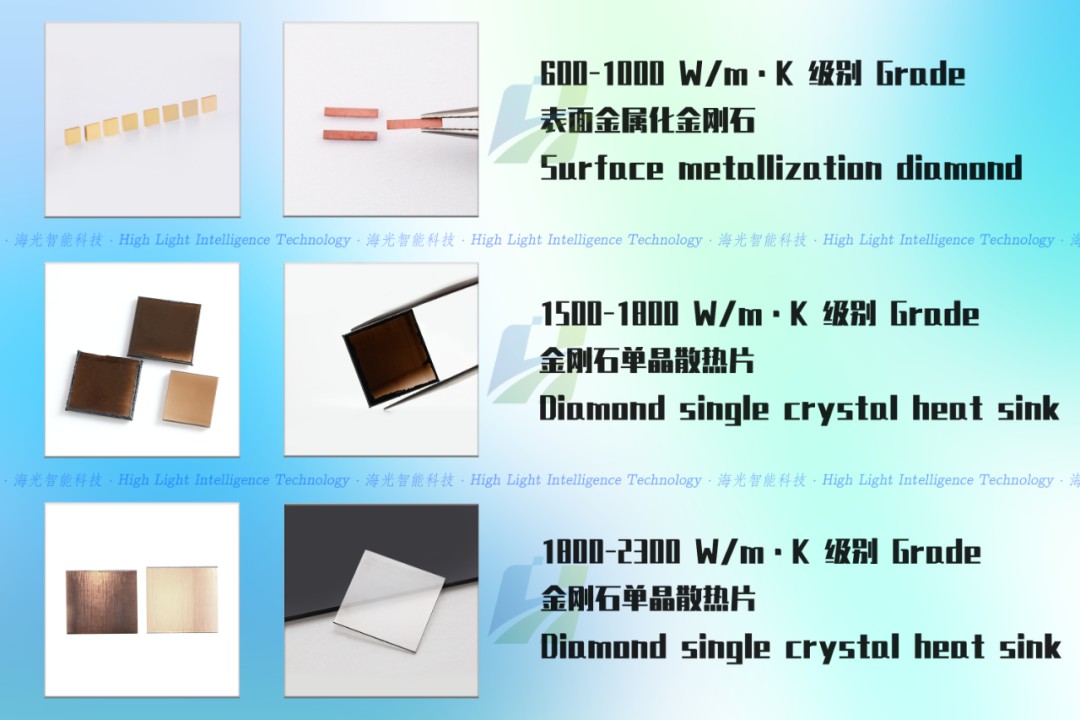

High Light Intelligence Technology, a pioneer in the CVD diamond industry, has advanced MPCVD technology and CVD diamond production workshops. We focus on producing high-purity lab-grown diamonds for the jewelry industry, and at the same time create industrial-grade CVD diamond products, covering single crystals, polycrystalline, films and diamond surface metallization. We also provide 6kw/10kw/15kw MPCVD equipment to help customers in all aspects, from equipment to products, and then to all-round services, to create brilliance together.
*The articles and pictures are only for industry communication and sharing. If there is any infringement, please contact us to delete them.









-

Foshan Highlight Intelligent Technology invites you to the 140th Canton Fair—join us at Booth 21.2A23-24 in the Friendship Hall to share in the brilliance.
Foshan Highlight Intelligent Technology invites you to the 140th Canton Fair—join us at Booth 21.2A23-24 in the Friendship Hall to share in the brilliance.
-
CVD Single-Crystal Diamonds: An Analysis of the Complete Processing Workflow from Gas-Phase Deposition to Finished Diamond Chips
MPCVD (Microwave Plasma Chemical Vapor Deposition) technology is currently the core process for producing high-quality single-crystal diamond s. Thanks to its advantages of low defect rates, high purity, and controllable large dimensions, it is widely used in fields such as semiconductor heat dissipation, precision optics, and high-end sensors. The final quality of single-crystal diamond s depends on comprehensive process control throughout the entire workflow—from vapor deposition growth to pos
-
Single-Crystal or Polycrystalline Diamond — Which Has Greater Potential?
As diamond continues to enter industries such as semiconductors, thermal management, optics, high-power electronics, and precision machining, the requirements for diamond materials are also evolving.
-
Diamond Polishing and Grinding Processes: Core Challenges and Industry Hurdles
Diamond is often hailed as the “ultimate material” – ranking 10 on the Mohs hardness scale, boasting an ultra‑high thermal conductivity (~2,200 W/(m·K)), excellent chemical stability, and broad optical transparency. These properties make it irreplaceable in cutting‑edge applications such as semiconductor heat dissipation, high‑end optics, and quantum chips. Yet the paradox of “good materials are hard to process” is nowhere more evident than in diamond. From rough grinding for planarization to at




