

- 中文
- English
- Español
Why Are Large-Size Single-Crystal Diamond Heat Sinks Manufactured Using a Mosaic Assembly Process?
2026-08-21 16:57:43
Click:
“
In the packaging design of 5G RF power amplifiers, automotive VCSEL radars, high-performance AI chips, and high-power industrial lasers, large-area single-crystal diamond heat sinks measuring 35 mm or larger are an essential requirement. Most procurement and thermal design engineers ask the same question: Why do 25×25 mm single-crystal heat sinks on the market tend to use a mosaic assembly structure? This is not due to a simplification of manufacturing processes, but rather because of unavoidabl
”
In the packaging design of 5G RF power amplifiers, automotive VCSEL radars, high-performance AI chips, and high-power industrial lasers, large-area single-crystal diamond heat sinks measuring 35 mm or larger are an essential requirement. Most procurement and thermal design engineers ask the same question: Why do 25×25 mm single-crystal heat sinks on the market tend to use a mosaic assembly structure? This is not due to a simplification of manufacturing processes, but rather because of unavoidable physical limitations in MPCVD single-crystal growth; the mosaic approach is currently the only industrial solution that balances high quality with mass-production feasibility.
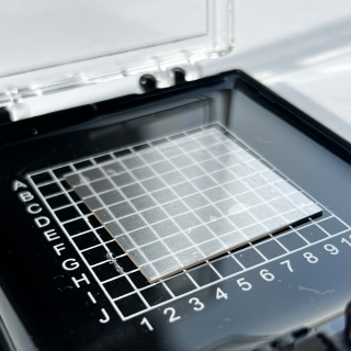
1. Limitations Imposed by the Uniform Temperature Zone in the Plasma Field
In mainstream 2450 MHz mass-production MPCVD systems, the microwave plasma is spherical. Only a very small central region within the chamber can maintain uniform and stable temperature, hydrocarbon gas flow, and plasma density. Only within this region can single-crystal diamond with low nitrogen content, no twins, and no polycrystalline regions be grown. If the seed crystal’s edge length exceeds 12 mm, the crystal edges fall within the region of plasma non-uniformity. The temperature gradient continues to widen, resulting in the growth of extensive polycrystalline layers and dislocation defects, causing a direct drop in local thermal conductivity of more than 30%. Even when using 915 MHz ultra-large-chamber equipment, the total cost of the system, energy consumption, and O&M costs increase by 8–10 times, with a yield rate of less than 10%, making industrial-scale batch production unfeasible.
2. Risk of Stress Cracking in Large-Area Crystal Growth
Diamond has an extremely low coefficient of thermal expansion. During the growth of a single large-size single crystal, a persistent temperature difference exists between the center and the edges of the crystal, causing massive internal growth stresses to accumulate. When the single crystal exceeds 25 mm in size, these stresses increase exponentially, making it highly prone to developing microscopic internal cracks invisible to the naked eye after cooling; under thermal cycling conditions in high-power devices, the entire single crystal may shatter, resulting in complete device failure. The mosaic process divides large crystals into multiple 10–12 mm standard, high-quality seed crystals, allowing the stress in each individual crystal to be controlled and eliminating the risk of hidden cracks at the source.
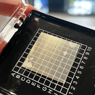
Many customers hold the misconception that assembly will compromise a heat sink’s thermal conductivity. In fact, a mature, precision mosaic assembly process fully preserves the core thermal dissipation advantages of single-crystal diamond, meeting the demands of high-end precision thermal management applications.
1. The overall thermal conductivity is excellent. The core heat dissipation areas of the heat sink consist entirely of high-purity single-crystal structures. The bonding interfaces undergo precise growth control, resulting in extremely low residual stress and preventing the formation of thermal barrier layers. The thermal conductivity of the entire substrate can be stably maintained at 1800–2000 W/m·K, which is essentially on par with that of a single, monolithic crystal and far exceeds that of traditional heat dissipation materials such as copper and silver.
2. Flatness and uniformity meet specifications. Through precise crystal orientation calibration, uniform thickness arrangement, and step-wise buffer growth, the large-size substrate achieved after joining exhibits high flatness and uniform thickness. After subsequent grinding and polishing, it can meet the large-area bonding requirements of chips and laser devices, ensuring gap-free bonding and effectively reducing interfacial thermal resistance.
3. They offer greater structural stability. The mosaic interfaces effectively block crack propagation. Compared to large, monolithic single crystals, which are highly brittle, mosaic-assembled heat sinks exhibit superior resistance to deformation and thermal shock, making them suitable for long-term operation under harsh conditions involving high power and extreme temperature cycling.

As a manufacturer with an in-house developed MPCVD full industrial chain, we are capable of mass-producing mosaic single-crystal heat sinks in sizes ranging from 35 to 100 mm. We offer customization options such as crystal orientation, ultra-thin reduction, and double-sided nano-polishing to provide a one-stop single-crystal diamond solution for the thermal management of high-power devices. If you have requirements for large-size single crystals, please feel free to consult our professional team.
High Light Intelligence Technology, a pioneer in the CVD diamond industry, has advanced MPCVD technology and CVD diamond production workshops. We focus on producing high-purity lab-grown diamonds for the jewelry industry, and at the same time create industrial-grade CVD diamond products, covering single crystals, polycrystalline, films and diamond surface metallization. We also provide 6kw/10kw/15kw MPCVD equipment to help customers in all aspects, from equipment to products, and then to all-round services, to create brilliance together.









-

CVD Single-Crystal Diamonds: An Analysis of the Complete Processing Workflow from Gas-Phase Deposition to Finished Diamond Chips
MPCVD (Microwave Plasma Chemical Vapor Deposition) technology is currently the core process for producing high-quality single-crystal diamond s. Thanks to its advantages of low defect rates, high purity, and controllable large dimensions, it is widely used in fields such as semiconductor heat dissipation, precision optics, and high-end sensors. The final quality of single-crystal diamond s depends on comprehensive process control throughout the entire workflow—from vapor deposition growth to pos
-
Single-Crystal or Polycrystalline Diamond — Which Has Greater Potential?
As diamond continues to enter industries such as semiconductors, thermal management, optics, high-power electronics, and precision machining, the requirements for diamond materials are also evolving.
-
Diamond Polishing and Grinding Processes: Core Challenges and Industry Hurdles
Diamond is often hailed as the “ultimate material” – ranking 10 on the Mohs hardness scale, boasting an ultra‑high thermal conductivity (~2,200 W/(m·K)), excellent chemical stability, and broad optical transparency. These properties make it irreplaceable in cutting‑edge applications such as semiconductor heat dissipation, high‑end optics, and quantum chips. Yet the paradox of “good materials are hard to process” is nowhere more evident than in diamond. From rough grinding for planarization to at
-
Single-Crystal vs Polycrystalline CVD Diamond: Process Difference Lies in Growth Logic, Not Equipment
The process difference between single crystal and polycrystalline CVD diamond lies not in equipment, but in growth logic. Single crystal and polycrystalline CVD diamond are two functional new materials with completely independent growth mechanisms, lattice structures and performance systems. Their process logic, product features and application boundaries diverge fundamentally from the very start of deposition and growth. Comparing or selecting materials without considering their underlying crys




