

- 中文
- English
- Español
Mosaic Single‑Crystal Diamond: Breaking Size Limits
2026-09-14 14:47:07
Click:
“
With an ultra‑wide bandgap of 5.47 eV, ultra‑high thermal conductivity (>2000 W/m·K), high carrier mobility (electron mobility up to 4500 cm²·V⁻¹·s⁻¹), and ultra‑high theoretical breakdown field strength (>10 MV/cm), Single‑Crystal Diamond (SCD) is an ideal candidate for next‑generation high‑power, high‑frequency and extreme‑environment electronic devices. However, both natural diamond and HPHT‑synthesized single‑crystal diamond are limited in lateral size, which greatly hinders large‑scal
”
With an ultra‑wide bandgap of 5.47 eV, ultra‑high thermal conductivity (>2000 W/m·K), high carrier mobility (electron mobility up to 4500 cm²·V⁻¹·s⁻¹), and ultra‑high theoretical breakdown field strength (>10 MV/cm), Single‑Crystal Diamond (SCD) is an ideal candidate for next‑generation high‑power, high‑frequency and extreme‑environment electronic devices. However, both natural diamond and HPHT‑synthesized single‑crystal diamond are limited in lateral size, which greatly hinders large‑scale industrial deployment.
The mosaic splicing method was developed to address this problem. High‑quality small‑size single‑crystal diamond seeds with uniform thickness and consistent crystal orientation are selected and assembled into a large‑area substrate. Microwave Plasma Chemical Vapor Deposition (MPCVD) is then applied for homoepitaxial growth, enabling lateral epitaxial fusion among adjacent seed crystals. The assembled substrate resembles mosaic tiles, hence the name “Mosaic splicing technology”. After growth, the splicing interface layer is removed to obtain large‑area single‑crystal diamond.

The manufacturing of mosaic single‑crystal diamond is a highly precise process, with key technical points as follows:
1. Seed Preparation and Splicing
High‑quality small‑size single‑crystal diamond seeds with consistent crystal orientation and uniform thickness are precisely assembled to form large‑area substrates. In recent years, side‑bonding technology has been developed: seed side surfaces are polished, contaminants are removed by Ar‑ion beam bombardment, bonding metal films are deposited, and seeds are pressed together for tight bonding, minimizing height differences across the substrate.
2. MPCVD Homoepitaxial Growth
The spliced substrate is loaded into an MPCVD reactor for homoepitaxial growth under optimized process parameters. The direction of step‑flow growth is controlled to achieve seamless merging of epitaxial layers from neighboring seeds. Research shows that co‑propagating growth fronts realize seamless epitaxial merging, while colliding growth fronts tend to generate polycrystalline defects.
3. Interface Quality Control
The core challenge of mosaic splicing lies in interface quality control. Through high‑precision crystal‑orientation matching (lattice orientation deviation within 1°), laser planarization and plasma etching, surface roughness can be reduced to 2.5 nm for greatly improved interface performance.

Mosaic single‑crystal diamond retains the intrinsic superior properties of single‑crystal diamond while achieving major breakthroughs in dimension:

For a 2×2 mosaic sample (18 mm × 18 mm), measured epitaxial strain ranges from (5.7–6.8)×10⁻⁴. The minimum X‑ray rocking‑curve FWHM reaches 0.0159° across quadrants. Good material continuity is maintained at splicing boundaries without unacceptable lattice defects. 214 Schottky diodes fabricated on the same wafer exhibit highly consistent electrical performance, with stable breakdown field above 2 MV/cm and RF performance up to 40 GHz.
Mosaic single‑crystal diamond delivers tremendous value in multiple cutting‑edge fields:
1. High‑Power Electronic Devices & Semiconductors
Single‑crystal diamond serves as an ideal substrate for high‑frequency and high‑power electronic devices. Mosaic splicing technology enables uniform fabrication of large‑area diamond Schottky barrier diode (SBD) arrays, laying a material foundation for mass production of wafer‑scale diamond SBD, PIN and RF devices.
2. Thermal Management
Boasting thermal conductivity up to 2200 W/m·K, among the highest of all known materials, diamond is regarded as the “ultimate solution” for semiconductor thermal management. Mosaic single‑crystal diamond has entered supply chains of leading enterprises, applied in thermal dissipation for AI servers, 5G base stations and new‑energy‑vehicle power modules.
3. Optical Windows & Detectors
Mosaic single‑crystal diamond shows great promise for infrared windows, high‑power laser windows and high‑energy‑particle detectors. 30×30×1 mm³ mosaic single‑crystal diamond infrared windows have been successfully manufactured.
4. Quantum Technology
Color centers in single‑crystal diamond such as the silicon‑vacancy (SiV⁻) center are critical carriers for quantum‑information platforms. Mosaic splicing interfaces can enhance SiV photoluminescence, opening new research directions for quantum sensing.
If you have a need for large-sized single-crystal diamond wafers, please contact us.

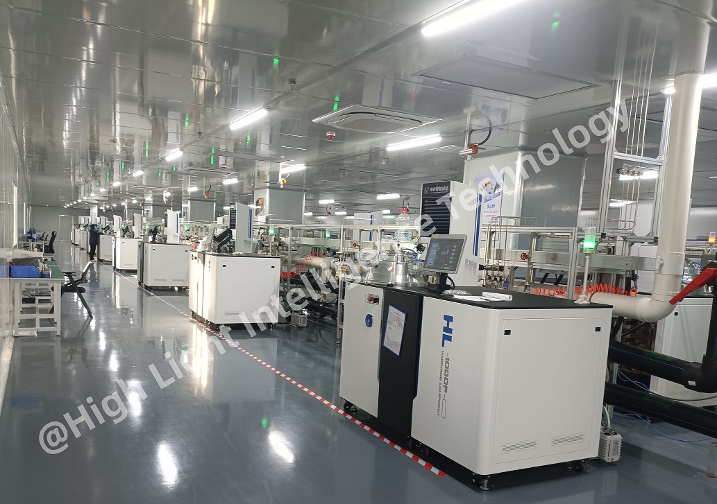
High Light Intelligence Technology, a pioneer in the CVD diamond industry, has advanced MPCVD technology and CVD diamond production workshops. We focus on producing high-purity lab-grown diamonds for the jewelry industry, and at the same time create industrial-grade CVD diamond products, covering single crystals, polycrystalline, films and diamond surface metallization. We also provide 6kw/10kw/15kw MPCVD equipment to help customers in all aspects, from equipment to products, and then to all-round services, to create brilliance together.









-

CVD Single-Crystal Diamonds: An Analysis of the Complete Processing Workflow from Gas-Phase Deposition to Finished Diamond Chips
MPCVD (Microwave Plasma Chemical Vapor Deposition) technology is currently the core process for producing high-quality single-crystal diamond s. Thanks to its advantages of low defect rates, high purity, and controllable large dimensions, it is widely used in fields such as semiconductor heat dissipation, precision optics, and high-end sensors. The final quality of single-crystal diamond s depends on comprehensive process control throughout the entire workflow—from vapor deposition growth to pos
-
Single-Crystal or Polycrystalline Diamond — Which Has Greater Potential?
As diamond continues to enter industries such as semiconductors, thermal management, optics, high-power electronics, and precision machining, the requirements for diamond materials are also evolving.
-
Diamond Polishing and Grinding Processes: Core Challenges and Industry Hurdles
Diamond is often hailed as the “ultimate material” – ranking 10 on the Mohs hardness scale, boasting an ultra‑high thermal conductivity (~2,200 W/(m·K)), excellent chemical stability, and broad optical transparency. These properties make it irreplaceable in cutting‑edge applications such as semiconductor heat dissipation, high‑end optics, and quantum chips. Yet the paradox of “good materials are hard to process” is nowhere more evident than in diamond. From rough grinding for planarization to at
-
Single-Crystal vs Polycrystalline CVD Diamond: Process Difference Lies in Growth Logic, Not Equipment
The process difference between single crystal and polycrystalline CVD diamond lies not in equipment, but in growth logic. Single crystal and polycrystalline CVD diamond are two functional new materials with completely independent growth mechanisms, lattice structures and performance systems. Their process logic, product features and application boundaries diverge fundamentally from the very start of deposition and growth. Comparing or selecting materials without considering their underlying crys



