

- 中文
- English
- Español
Direct bonding of diamond and semiconductor
2023-12-01 09:06:38
Click:
In recent years, with the rapid development of electronic devices, the thermal conductivity of traditional materials has been unable to meet the heat dissipation needs of high-power density chips. In order to effectively remove the heat generated by device operation and ensure the continued smooth operation of the system, new high thermal conductivity materials have been developed. Development and application have become hot topics at the moment.
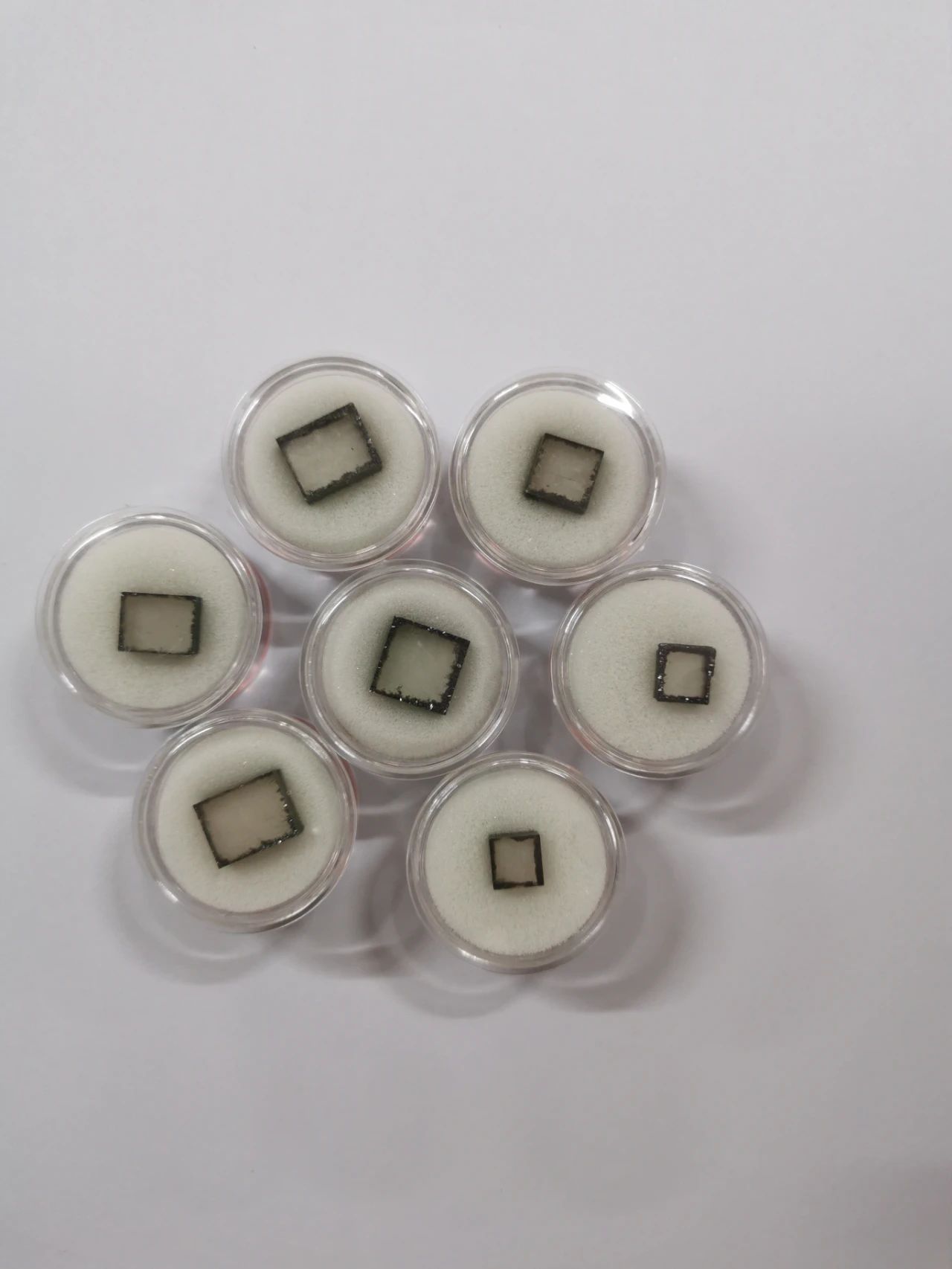
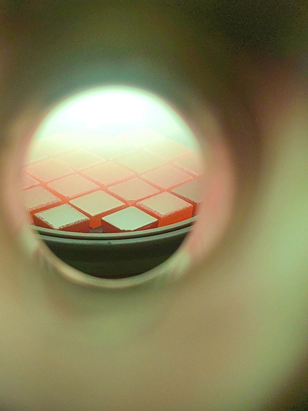
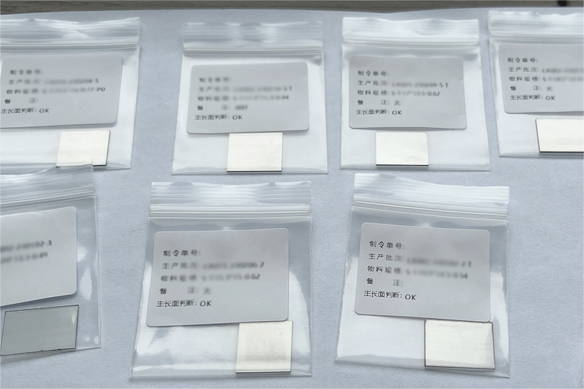
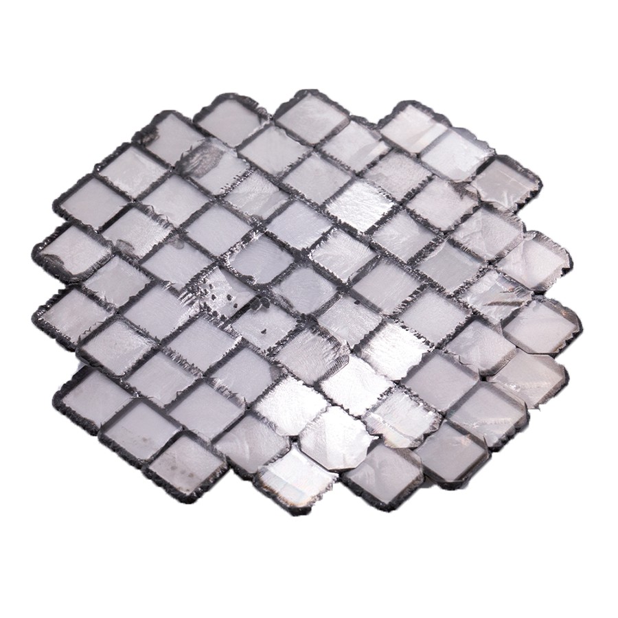
Diamond is a very competitive heat dissipation material with a thermal conductivity as high as 2000W/ (m·k), while the thermal conductivity of Si is 150W/ (m·k) and that of Cu is 380W/ (m·k) ), which means that diamond materials can transfer heat more effectively and improve the operating efficiency and using time of integrated circuits. In addition, diamond has a higher breakdown voltage (10 MV/cm) than the semiconductor materials Si (≈0.3 MV/cm), SiC (≈3 MV/cm), and GaN (≈10 MV/cm) , which represents extremely high electrical insulation and is conducive to the miniaturization of devices.
Therefore, using diamond sheets or films as heat sinks to improve the heat dissipation capabilities of semiconductor devices has become a widely recognized heat dissipation treatment solution. Based on diamond's efficient heat dissipation capabilities, it reduces the thermal stress generated under high-power operation and ensures that the material able to run at higher power without overheating. However, due to the lattice mismatch caused by thermal expansion and high pressure between the diamond substrate and the semiconductor device, the yield of the material is greatly reduced. To realize the large-scale application of diamond in the semiconductor field, the first thing to solve is the problem of diamond and semiconductor. Connection issues.
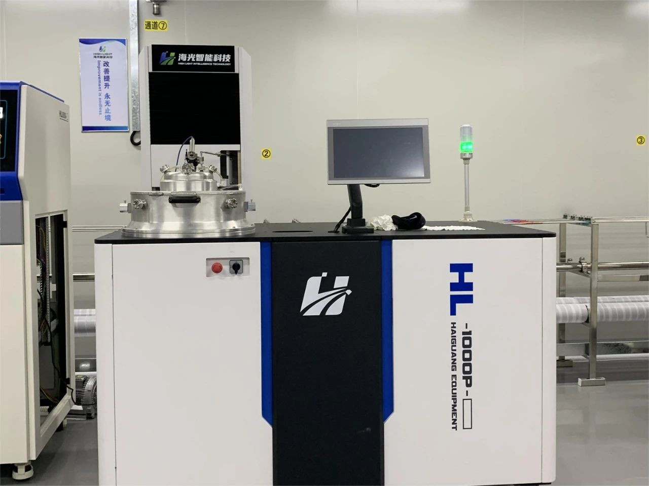
The direct bonding between diamond and semiconductor can give full play to the ultra-high thermal conductivity of diamond. However, this has higher requirements on the flatness and roughness of the diamond surface. Usually the surface roughness reaches Ra<1 nm. Limited by the synthesis mechanism of diamond, the roughness of the diamond surface often increases to tens of microns. Therefore, more sophisticated processing methods must be used to reduce the roughness of the diamond surface to the nanometer level and improve surface accuracy to achieve bonding Require.
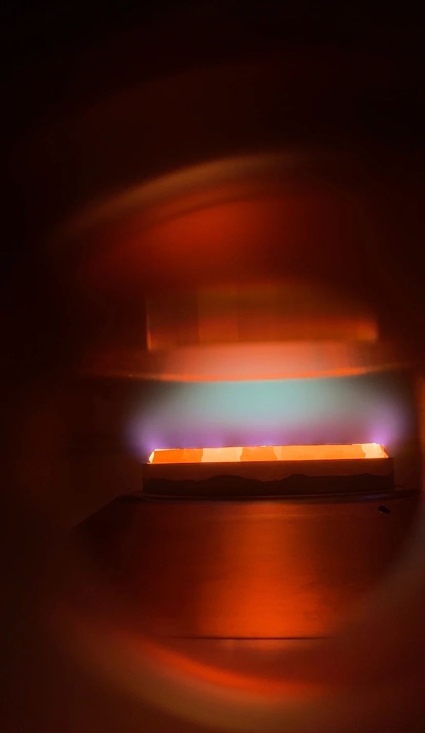
With MPCVD technology as its core, High Light Intelligence Technology has long been committed to the R&D and manufacturing of high-quality diamond materials and related equipment. It has advanced MPCVD equipment, laser processing equipment and precision polishing equipment. For diamond surface polishing, our company uses mechanical polishing to ensure high efficiency, high precision, and low damage. At the same time, we can process the surface roughness of diamond growth to the nanometer level, greatly reducing the surface roughness value (Ra < 0.5 nm) and has extremely high surface accuracy, which expands the contact area and greatly improves the yield and reliability of the direct bonding process.









-

CVD Single-Crystal Diamonds: An Analysis of the Complete Processing Workflow from Gas-Phase Deposition to Finished Diamond Chips
MPCVD (Microwave Plasma Chemical Vapor Deposition) technology is currently the core process for producing high-quality single-crystal diamond s. Thanks to its advantages of low defect rates, high purity, and controllable large dimensions, it is widely used in fields such as semiconductor heat dissipation, precision optics, and high-end sensors. The final quality of single-crystal diamond s depends on comprehensive process control throughout the entire workflow—from vapor deposition growth to pos
-
Single-Crystal or Polycrystalline Diamond — Which Has Greater Potential?
As diamond continues to enter industries such as semiconductors, thermal management, optics, high-power electronics, and precision machining, the requirements for diamond materials are also evolving.
-
Diamond Polishing and Grinding Processes: Core Challenges and Industry Hurdles
Diamond is often hailed as the “ultimate material” – ranking 10 on the Mohs hardness scale, boasting an ultra‑high thermal conductivity (~2,200 W/(m·K)), excellent chemical stability, and broad optical transparency. These properties make it irreplaceable in cutting‑edge applications such as semiconductor heat dissipation, high‑end optics, and quantum chips. Yet the paradox of “good materials are hard to process” is nowhere more evident than in diamond. From rough grinding for planarization to at
-
Single-Crystal vs Polycrystalline CVD Diamond: Process Difference Lies in Growth Logic, Not Equipment
The process difference between single crystal and polycrystalline CVD diamond lies not in equipment, but in growth logic. Single crystal and polycrystalline CVD diamond are two functional new materials with completely independent growth mechanisms, lattice structures and performance systems. Their process logic, product features and application boundaries diverge fundamentally from the very start of deposition and growth. Comparing or selecting materials without considering their underlying crys




