

- 中文
- English
- Español
Another big announcement! Diamonds used as chips
2023-12-01 09:18:42
Click:
why diamonds ?
Diamond is an ultra-broadband semiconductor with the highest thermal conductivity, which is a ability to transfer heat of material. Because of these properties, diamond semiconductor devices can operate at higher voltages and currents (using less material) than traditional semiconductor materials such as silicon, and still dissipate heat without causing degradation in electrical performance."To have a grid that requires high currents and high voltages to make applications like solar panels and wind turbines more efficient, then we need a technology that doesn't have thermal limitations. That's where diamonds come in," Bayram said .
Although many people associate diamonds with expensive jewelry, diamonds can be made more economically and sustainably in laboratories, making them a viable and important semiconductor alternative. Natural diamonds are formed deep under the Earth's surface under immense pressure and heat, but since it is essentially just carbon (which is abundant), so synthetic diamonds can be made in weeks instead of billions of years , while it also reduces carbon emissions by 100 times.
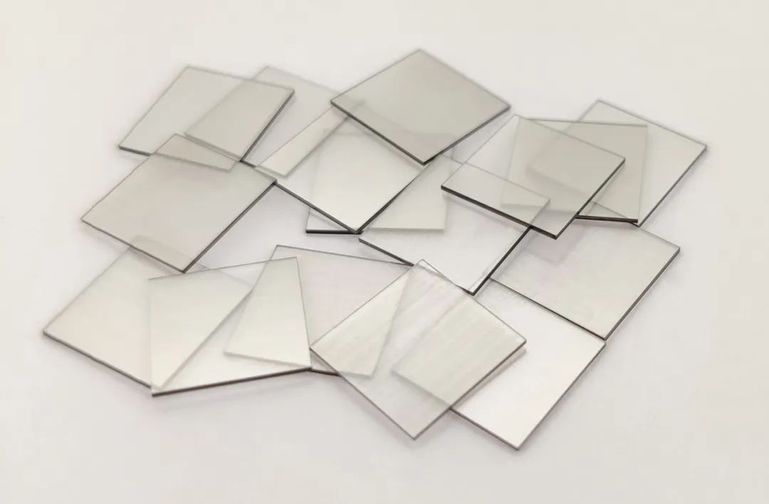
In this work, Bayram and Han showed that their diamond device can withstand high voltages of approximately 5 kV, although the voltage is limited by the measurement setup rather than from the device itself. Theoretically, the device can withstand voltages up to 9kV. This is the highest voltage reported by a diamond device. In addition to the highest breakdown voltage, the device also exhibits the lowest leakage current and can be thought of as a leaky faucet with energy. Leakage current affects the overall efficiency and reliability of the device."We built an electronic device that is better suited for high-power, high-voltage applications in future grids and other electric power applications," Han said. "We built the device on an ultra-wide-bandgap material, synthetic diamond, which promises higher efficiencies." and better performance." "Performance is better than the current generation of devices. Hopefully we can continue to optimize this device and other configurations so that we can approach the performance limits of the diamond material's potential."
The following is the original text of the paper:
Diamond p-type lateral Schottky barrier diode with high breakdown voltage (4612V at 0.01mA/Mm)
Introduction
Diamond is an emerging semiconductor for high-power electronics with its large bandgap (EG, 5.47 eV), large critical E-field (EB, 10 – 20 MV/cm), high carrier mobility (μ , up to 2100 cm2⋅ V−1⋅ s−1 for holes at low doping concentrations (<1015 cm−3)), and high thermal conductivity (k, 22 - 24 W⋅ cm−1⋅K−1 ) [1]. The relatively low activation energy of p-type boron dopants (0.38 eV compared to 0.57 eV for n-type phosphorus) and the maturation of CVD grown boron-doped diamond motivate p-type diamond Schottky diodes for studies [2] and high critical fields of 7.7 MV/cm [3] and breakdown voltages of 2.5 kV [4] have been demonstrated in either vertical or pseudo-vertical configurations. Increasing the breakdown voltages higher in these devices require increasing the drift layer thickness [5], which is challenging to grow experimentally [6], [7], as well as etching deeper, which creates processing issues [8]. One way to scale diamond SBD to higher voltage is using their lateral configuration, where breakdown voltages are scaled via adjusting the distance between the anode and cathode, without the need for a thick drift layer.
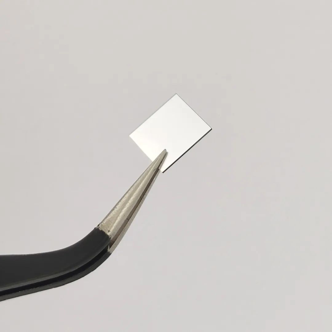
In this letter, diamond p-type lateral Schottky barrier diodes (SBDs) with high breakdown voltage (4612 V) enabled with contact regrowth and edge termination techniques are reported. Forward I-V characteristics are studied using the thermionic emission model and the Mott-Gurney relation. The SBDs are simulated under reverse bias using Synopsys’ Sentaurus TCAD software to investigate the effect of the field plate structures. The simulation predicts a significant reduction in the peak electric field with the addition of the field plate, which agrees with the breakdown performance of diodes with and without the field plate measured by experiments. Finally, the lateral SBDs are benchmarked against previously reported diamond power devices in terms of specific on-resistance (RON) and breakdown voltage (Vbr).
Device Fabrication
Fig. 1 shows the epitaxy (by microwave plasma enhanced chemical vapor deposition (MPCVD)) and cleanroom microfabrication process flow of diamond p-type lateral SBDs. First, a
Fig. 1. Epitaxy and cleanroom microfabrication steps for diamond lateral SBDs (a)
Results and Discussion
Fig. 2(a) shows the semi-logarithmic and linear (inset) J-V curves of fabricated diamond p-type lateral SBD with and without the Al2O3 field plate at room temperature. The SBD without the field plate has the same Schottky to ohmic distance
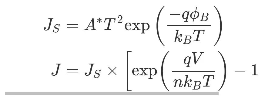
where
Fig. 2.(a) Forward J-V characteristics of diamond lateral SBD with and without the field plate (FP) in semi-logarithmic and (inset) linear scales at room temperature (RT); the dashed line represents the calculated space charge limited conduction (SCLC) J-V relation. (b) Forward J-V characteristics of diamond lateral SBD with and without the FP in semi-logarithmic and (inset) linear scales at 200 °C.
Fig. 2(a) also plots the calculated space charge limited conduction (SCLC) current density for 10 – 40V forward voltages in the fabricated diodes. Due to dopants incomplete ionization at room temperature, the active hole concentration in the drift region is estimated to be lower than 1014 cm−3. As the applied forward bias increases, charge neutrality is no longer maintained as injected charges accumulate in the drift region, and the SCLC begins to dominate [14]. For a lightly doped semiconductor, the SCLC is described by the Mott-Gurney relation:
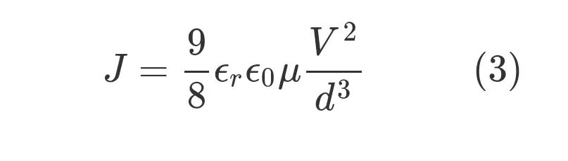
where
Fig. 3. Room temperature reverse leakage J-V characteristics of diamond lateral SBD with and without the FP.
Fig. 4 shows the simulated horizontal electric field magnitude along the dashed cutlines at
Fig. 4. Simulated horizontal electric field magnitude along the dashed cutlines at 0.1 μm
Fig. 5 shows a benchmark of specific on-resistance (RON) vs. breakdown voltage (Vbr) at room temperature. This work exhibits a higher breakdown voltage than previously reported pseudo-vertical and vertical SBDs, lateral MESFETs, MOSFETs, and JEFTs.
Fig. 5. Benchmark of the fabricated lateral SBDs compared with previously reported diamond power devices including lateral MESFETs, MOSFETs and junction FETs, and pseudo-vertical and vertical SBDs at room temperature. The leakage currents at which the breakdown is reported are shown in the brackets.
The specific on-resistances are normalized to be
Conclusion
In conclusion, diamond p-type lateral SBDs with and without the Al2O3 field plate are reported. At room temperature, the diodes exhibit a rectifying ratio of 107 and have forward current densities of 0.049 (with field plate) and 0.044 (without field plate) mA/mm at 40 V forward bias. The specific on-resistances are 534 (without field plate) and 527 (with field plate)









-

CVD Single-Crystal Diamonds: An Analysis of the Complete Processing Workflow from Gas-Phase Deposition to Finished Diamond Chips
MPCVD (Microwave Plasma Chemical Vapor Deposition) technology is currently the core process for producing high-quality single-crystal diamond s. Thanks to its advantages of low defect rates, high purity, and controllable large dimensions, it is widely used in fields such as semiconductor heat dissipation, precision optics, and high-end sensors. The final quality of single-crystal diamond s depends on comprehensive process control throughout the entire workflow—from vapor deposition growth to pos
-
Single-Crystal or Polycrystalline Diamond — Which Has Greater Potential?
As diamond continues to enter industries such as semiconductors, thermal management, optics, high-power electronics, and precision machining, the requirements for diamond materials are also evolving.
-
Diamond Polishing and Grinding Processes: Core Challenges and Industry Hurdles
Diamond is often hailed as the “ultimate material” – ranking 10 on the Mohs hardness scale, boasting an ultra‑high thermal conductivity (~2,200 W/(m·K)), excellent chemical stability, and broad optical transparency. These properties make it irreplaceable in cutting‑edge applications such as semiconductor heat dissipation, high‑end optics, and quantum chips. Yet the paradox of “good materials are hard to process” is nowhere more evident than in diamond. From rough grinding for planarization to at
-
Single-Crystal vs Polycrystalline CVD Diamond: Process Difference Lies in Growth Logic, Not Equipment
The process difference between single crystal and polycrystalline CVD diamond lies not in equipment, but in growth logic. Single crystal and polycrystalline CVD diamond are two functional new materials with completely independent growth mechanisms, lattice structures and performance systems. Their process logic, product features and application boundaries diverge fundamentally from the very start of deposition and growth. Comparing or selecting materials without considering their underlying crys




