

- 中文
- English
- Español
Diamond chips are about to be commercialized
2024-06-07 10:26:15
Click:
“
Diamond has emerged in the semiconductor industry in recent years and has become the focus of the industry. In order to achieve decarbonization, the industry strives for more advanced semiconductor technology. Breakthroughs in materials such as gallium nitride and silicon carbide have helped the industry surpass the limitations of silicon and are widely used in carbon reduction technologies such as renewable energy and electric vehicles. As an emerging semiconductor material, diamond is world-r
”
Diamond has emerged in the semiconductor industry in recent years and has become the focus of the industry. In order to achieve decarbonization, the industry strives for more advanced semiconductor technology. Breakthroughs in materials such as gallium nitride and silicon carbide have helped the industry surpass the limitations of silicon and are widely used in carbon reduction technologies such as renewable energy and electric vehicles. As an emerging semiconductor material, diamond is world-renowned for its hardness and brightness. It was once mainly used in jewelry, but now its characteristics show great potential in the semiconductor field and have attracted much attention.

As a semiconductor material, diamond has three major advantages: excellent thermal management, cost/efficiency optimization, and environmental protection and emission reduction. Its resistivity decreases with increasing temperature, so it performs better at 150°C without the need for a complex cooling system. Diamond has excellent heat dissipation properties, making the converter lightweight, small and efficient. In applications such as electric vehicles, diamond can significantly reduce costs, increase efficiency, and reduce size and weight. Compared to silicon carbide, diamond chips are less expensive, more energy efficient, smaller and have better thermal management. Diamond will play an important role in energy-saving fields such as electric vehicles, and the market potential is huge.


Diamond has extremely high insulation properties, with a breakdown electric field strength of 10 MV/cm, far exceeding that of silicon, SiC and GaN. Its excellent thermal conductivity makes it suitable for heat dissipation of 5G components to ensure stable operation. Diamond substrates combined with gallium nitride or silicon carbide can be used to manufacture high-efficiency power devices, which are widely used in electric vehicles, renewable energy and other fields. As high-quality heat sinks, diamond substrates extend equipment life and improve reliability. With the advancement of clean energy and automotive electrification, diamond substrates will play a key role. The diamond semiconductor substrate market was valued at US$151 million in 2023 and is expected to reach US$342 million by 2030, with the Asia-Pacific region dominating the market.
Although high-performance semiconductor materials are superior, they face limitations such as high cost and small size of diamond wafers. The cost of silicon carbide is 30-40 times that of silicon, gallium nitride is as high as 650-1300 times, and the price of diamond materials is 10,000 times that of silicon. To overcome these limitations, many companies are working on diamond mass production technology. Saga University in Japan and Orbray successfully manufactured 2-inch diamond power semiconductors, and Diamond Foundry in the United States manufactured single-crystal diamond wafers with a diameter of about 4 inches. French Diamfab has also made progress in diamond chip technology. In March this year, it received a first round of financing of 8.7 million euros, supported by investors such as Asterion Ventures and the French government. Diamfab was derived from the Nair Institute of the French National Center for Scientific Research (CNRS) and was founded by two nanoelectronics doctors and researchers.
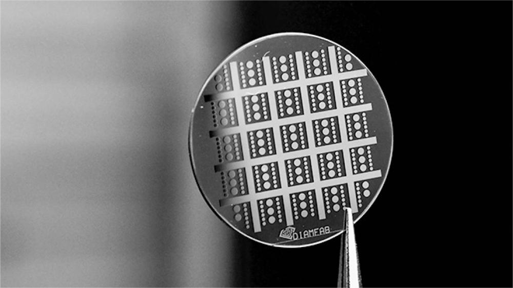
Diamfab has made breakthroughs in diamond epitaxy and doping technology, owns four patents, and focuses on diamond layer growth, doping and electronic component design. The first round of financing will help it establish a pilot production line and accelerate the industrialization of diamond semiconductor technology. Diamfab's diamond technology achieves high current density and breakdown electric field, surpassing existing materials such as SiC, and plans to achieve 4-inch wafer production in 2025. CEO Gauthier Chicot emphasized the importance of cooperation with partners and reducing the carbon footprint of semiconductors. Another startup, Advent Diamond, focuses on mass production of diamond semiconductors. It is the only company that can grow single-crystal phosphorus-doped diamond on a substrate, has achieved the manufacture of n-type semiconductors, and has made progress in growing boron-doped diamond layers over large areas. It has comprehensive component design, manufacturing and characterization capabilities.

Advent Diamond develops diamond radiation detectors, bringing changes to the defense, commercial and scientific markets. The detectors show excellent performance through doping and intrinsic diamond layers, and are suitable for a variety of radiation. Faced with challenges in wafer size and defects, but received institutional funding to promote technological development. Committed to innovation in diamond semiconductor performance, promoting the development of electrification, telecommunications and quantum fields. Akhan Semiconductor uses cryogenic technology to break the limitations of diamond use, successfully creates n-type diamond materials, and develops the Miraj Diamond platform. CMOS silicon is combined with diamond substrates to make 300 mm wafers. This year, a new company Diamond Quanta was established to focus on the semiconductor field. Its "unified diamond frame" technology transforms diamond into high-performance semiconductors, which is expected to redefine performance standards and meet the needs of modern industry.


Despite the high domestic diamond production, it still lags behind in functional applications and material development. Wang Dong, deputy director of the Wuhu Research Institute of Xidian University, pointed out that the domestic diamond industry is large but not strong, and lags behind in high-end fields. In CVD diamond research, the United States, Europe, and Japan are leading, and my country has little original research. Although there are challenges in the mass production and commercial use of diamonds around the world, the excellent properties of diamond materials are expected to promote important progress in the field of semiconductor materials in the future.
*The article is only for industry communication and sharing. If it involves infringement, please contact us to delete it.


-

Z-Axis System: The Key to Stable Production of MPCVD Diamonds
Microwave Plasma Chemical Vapor Deposition is the mainstream method for producing high-quality diamonds in the industry. When the equipment is running, it first pumps the reaction chamber into a vacuum state to strictly ensure the chamber is fully sealed and airtight. Then, the microwave device releases energy, and special mixed reaction gases are fed into the chamber. Under the action of energy, a stable plasma area is formed. These highly active plasmas provide stable heat and reaction conditi
-
How to Choose the Right MPCVD Equipment?
MPCVD equipment is a critical asset across a wide range of industries, including industrial manufacturing, semiconductor thermal management, precision cutting tools, and lab-grown diamonds. Choosing the right equipment not only boosts production efficiency and ensures consistent product quality but also effectively controls long-term costs, making your entire production process smoother and more competitive. Many people struggle with the question: How do I make the right choice? Today, drawing o
-
CVD Diamond Clarity: How to Avoid Inclusions That Affect Jewelry Value
After selecting a loose diamond, the setting not only determines the diamond’s security but also directly affects its perceived size. With diamonds of the same weight, choosing the right setting design can effortlessly create the surprise of “small carats making a big impact,” saving on your budget while enhancing the diamond’s quality. Among these, pavé and prong settings are the two most classic and effective ways to make a diamond appear larger. Paired with specialized designs that maximize t
-
How Diamond Became the Ultimate Thermal Solution in the Era of Computing Power
The iconic narrative behind the legendary "A Diamond is Forever" slogan has long been upended by China's industrial prowess. Once synonymous with luxury and rarity, this gem has shed its glamorous aura to become an indispensable thermal management material for high-power devices. In an era of explosive growth in AI computing power, it has taken up the mantle of "cooling to save computing power".


