

- 中文
- English
- Español
Why do CVD diamond wafers need to be polished?
2024-03-13 10:20:22
Click:
“
It is packaged in a small dark box with only a few pins exposed. The chip will look at the threshold value, resistance value, current value, and voltage value, but no one will see its appearance. We polish the CVD diamond wafer repeatedly during the manufacturing process. In order to meet the flattening needs in production, especially every time when doing photolithography, the surface of the CVD diamond wafer must be extremely flat. This is because as the chip manufacturing process shrinks, the
”
It is packaged in a small dark box with only a few pins exposed. The chip will look at the threshold value, resistance value, current value, and voltage value, but no one will see its appearance. We polish the CVD diamond wafer repeatedly during the manufacturing process. In order to meet the flattening needs in production, especially every time when doing photolithography, the surface of the CVD diamond wafer must be extremely flat. This is because as the chip manufacturing process shrinks, the lens of the photolithography machine must achieve nanoscale To improve the imaging resolution, we must desperately increase the numerical aperture (Numerical Aperture) of the lens, but this will also lead to a decrease in the depth of focus (DoF). The depth of focus refers to the depth of focus of optical imaging. To ensure that the lithography image is clear and clear To focus, the undulations on the CVD diamond wafer surface must fall within the focus depth range.
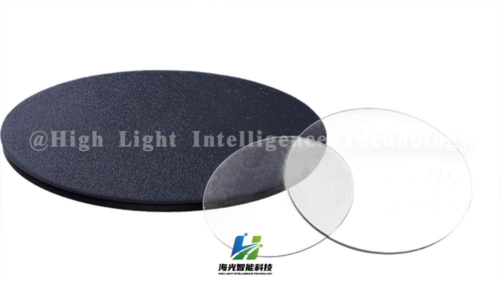
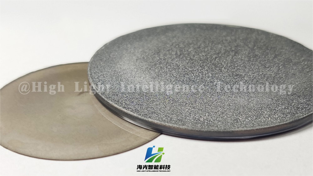
Therefore, the birth of a chip requires many times of polishing to reduce the roughness and undulations of the CVD diamond wafer, and to remove excess material on the surface. In addition, surface defects caused by various process problems on the CVD diamond wafer often have to wait until It will be exposed only after each grinding is completed, so the engineers responsible for grinding have a heavy responsibility. They are not only the C position that connects the previous and the next in the chip manufacturing process, but also the T position that takes the blame during the production meeting. They must be able to wet etch and You have to understand the physical output, because the chip factory is the most important polishing technology.
What are the polishing methods
for
CVD diamond wafers?
1
Mechanical polishing method
Mechanical polishing is a polishing method that relies on cutting and plastic deformation of the material surface to remove the polished convex parts to obtain a smooth surface. Generally, oilstone strips, wool wheels, sandpaper, etc. are used, and the operation is mainly manual. Special parts such as the surface of the rotary body can be Using auxiliary tools such as turntables, ultra-precision grinding and polishing methods can be used if the surface quality is high. Super-precision polishing uses special abrasives, which are pressed against the surface of the workpiece to be processed in a polishing fluid containing abrasives to perform high-speed rotation. This technology can achieve a surface roughness of Ra0.008μm, which is the highest among various polishing methods. This method is often used for optical lens molds.
2
Chemical polishing method
Chemical polishing is to allow the microscopic convex parts of the surface of the material to be dissolved preferentially in the chemical medium than the concave parts, thereby obtaining a smooth surface. The main advantage of this method is that it does not require complex equipment, can polish workpieces with complex shapes, and can polish many workpieces at the same time, with high efficiency. The core issue of chemical polishing is the preparation of polishing fluid. The surface roughness obtained by chemical polishing is generally several 10 μm.
3
Chemical mechanical polishing method
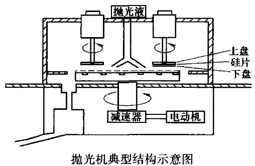
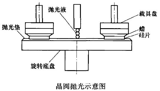
The first two polishing methods have their own unique advantages. If these two methods are combined, the advantages and disadvantages of the process can be complementary. Chemical mechanical polishing uses a process that combines mechanical friction and chemical corrosion. During the CMP working process, the chemical reagents in the polishing fluid used in CMP will oxidize the base material to be polished, forming a soft oxide film layer, and then The oxide film is removed through mechanical friction, and the purpose of effective polishing is achieved through repeated oxidation film formation-mechanical removal processes.
1. Process consistency :
Achieving a high degree of consistency in CMP processes remains a challenge. Even on the same production line, there may be small differences in process parameters between batches or between different equipment, affecting the consistency of the final product.
2. New material adaptability:
As new materials continue to emerge, CMP technology needs to continuously adapt to the characteristics of new materials. Some advanced materials may not be compatible with traditional CMP processes, and more adaptable polishing fluids and abrasives need to be developed.
3. Size effect:
As the size of semiconductor devices continues to shrink, the problems caused by size effects have become more significant. At micro sizes, surface flatness requirements are higher, so a more precise CMP process is required
4. Material removal rate control:
In some applications, precise removal rate control of different materials becomes particularly critical. Ensuring consistent removal rates of different layers of materials during the CMP process is critical to fabricating high-performance devices.
5. Environmentally friendly:
The polishing fluids and abrasives used in the CMP process may contain some environmentally harmful ingredients. Researching and developing more environmentally friendly and sustainable CMP processes and materials is an important challenge.
6. Intelligence & automation:
CMP systems are gradually becoming more intelligent and automated, but they still need to cope with complex and ever-changing production environments. How to achieve a higher degree of automation and intelligent monitoring to improve production efficiency is a problem that needs to be solved.
7. Cost control:
The CMP process involves high equipment and material costs. Manufacturers need to strive to reduce production costs while improving process performance to maintain market competitiveness.









-

CVD Single-Crystal Diamonds: An Analysis of the Complete Processing Workflow from Gas-Phase Deposition to Finished Diamond Chips
MPCVD (Microwave Plasma Chemical Vapor Deposition) technology is currently the core process for producing high-quality single-crystal diamond s. Thanks to its advantages of low defect rates, high purity, and controllable large dimensions, it is widely used in fields such as semiconductor heat dissipation, precision optics, and high-end sensors. The final quality of single-crystal diamond s depends on comprehensive process control throughout the entire workflow—from vapor deposition growth to pos
-
Single-Crystal or Polycrystalline Diamond — Which Has Greater Potential?
As diamond continues to enter industries such as semiconductors, thermal management, optics, high-power electronics, and precision machining, the requirements for diamond materials are also evolving.
-
Diamond Polishing and Grinding Processes: Core Challenges and Industry Hurdles
Diamond is often hailed as the “ultimate material” – ranking 10 on the Mohs hardness scale, boasting an ultra‑high thermal conductivity (~2,200 W/(m·K)), excellent chemical stability, and broad optical transparency. These properties make it irreplaceable in cutting‑edge applications such as semiconductor heat dissipation, high‑end optics, and quantum chips. Yet the paradox of “good materials are hard to process” is nowhere more evident than in diamond. From rough grinding for planarization to at
-
Single-Crystal vs Polycrystalline CVD Diamond: Process Difference Lies in Growth Logic, Not Equipment
The process difference between single crystal and polycrystalline CVD diamond lies not in equipment, but in growth logic. Single crystal and polycrystalline CVD diamond are two functional new materials with completely independent growth mechanisms, lattice structures and performance systems. Their process logic, product features and application boundaries diverge fundamentally from the very start of deposition and growth. Comparing or selecting materials without considering their underlying crys




